Spacer discharging apparatus and method of field emission display

Inactive Publication Date: 2005-01-20
LG ELECTRONICS INC
View PDF3 Cites 3 Cited by
  • Summary
  • Abstract
  • Description
  • Claims
  • Application Information

AI Technical Summary

Benefits of technology

[0029] Therefore, an object of the present invention is to provide a spacer discharging apparatus and method of an FED (Field Emission Display) capable of preventing generation of noise on a screen by controlling a discharge path, which selectively connects an anode electrode and a spacer ground electrode of the FED.

Problems solved by technology

However, the conventional FED does not have a discharge path for discharging electric charge charged on the spacer 104, so a noise is generated with the image displayed on the screen for a certain time while the electric charge charged on the spacer 104 is being discharged.
As shown in FIG. 3, the change of the voltage applied to the anode electrode of the conventional FED indicates that even after the high voltage applied to the anode electrode 102 is cut off or power applied to the scan electrode 107A is cut off, the voltage or the power is gradually reduced for a certain time, so that there is a high possibility that noise generated on the screen.
That is, since the electrons discharged from the cathode electrode collide with and are accumulated in the spacer, noise is generated on the screen.

Method used


Image

  • Spacer discharging apparatus and method of field emission display
  • Spacer discharging apparatus and method of field emission display
  • Spacer discharging apparatus and method of field emission display

Examples


first embodiment

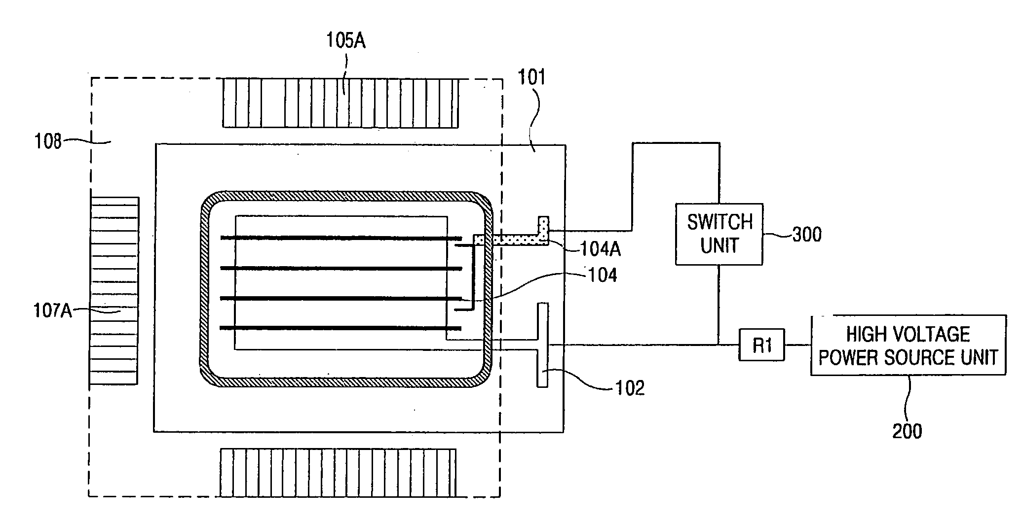
[0053]FIG. 6 is a schematic view showing a spacer discharging apparatus of an FED in accordance with the present invention.

[0054] As shown in FIG. 6, the spacer discharging apparatus of the FED in accordance with the first embodiment of the present invention includes: a spacer 104 that can be represented as an equivalent circuit in which a resistance component (Rs) and a capacitance component (Cs) are connected in parallel; an anode electrode 102 connected to an upper end portion of the spacer 104; a spacer ground electrode 104A connected to a lower end portion of the spacer 104; a first resister R1 connected between the anode electrode 102 and the high voltage power source unit 200; and a switch SW1 connected to the resister R1 and selectively connecting the anode electrode 102 and the spacer ground electrode 104A.

[0055] In the spacer discharging apparatus of the FED in accordance with the first embodiment of the present invention, when a scan voltage applied to the scan electrode...

second embodiment

[0057]FIG. 7 is a schematic view showing a spacer discharging apparatus of an FED in accordance with the present invention.

[0058] As shown in FIG. 7, a spacer discharging apparatus of an FED in accordance with the second embodiment of the present invention additionally includes a second resister R2 for controlling discharge time between the switch SW1 and the spacer ground electrode to the spacer discharging apparatus of the FED in accordance with the first embodiment of the present invention.

[0059] The second resister R2 is to be positioned between the anode electrode 102 and the spacer ground electrode 104A, so it can be positioned between the switch SW1 and the spacer ground electrode 104A or between the anode electrode 102 and the switch SW1.

[0060] In the spacer discharging apparatus of the FED in accordance with the second embodiment of the present invention, since the second resister R2 is positioned on the discharge path between the anode electrode 102 and the spacer ground...


PUM


Abstract

A spacer discharging apparatus and method of a field emission display (FED) are disclosed. The spacer discharging apparatus of an FED includes a first resister connected between an anode electrode of the FED and a high voltage power source unit applying a high voltage to the anode electrode, and a switch unit connected to the anode electrode and the first resister and selectively connecting the anode electrode and the spacer ground electrode of the FED.

Description

BACKGROUND OF THE INVENTION [0001] 1. Field of the Invention [0002] The present invention relates to a field emission display (FED) and more particularly, to a spacer discharging apparatus and method of a field emission display (FED). [0003] 2. Description of the Background Art [0004] In general, as the information processing systems are developed and widely spread, a display device as a time information transmission means has increasing importance. Of display devices, researches are actively ongoing on a flat panel display such as a liquid crystal display (LCD), a plasma display panel (PDP) and the FED or the like, to accomplish a large screen, flatness, high luminance and high efficiency. [0005] Especially, the FED, which is anticipated to be commercialized in the near future, receives much attention as a flat panel display for a next-generation information communications, which overcomes shortcomings of the flat display devices. [0006] The FED includes a front substrate having a ...

Claims


Application Information

Patent Timeline
IPC IPC(8): H01J9/02G09G3/22
CPCG09G3/22G09G2330/027G09G2310/061H01J9/02
Inventor MOON, SEONG HAK
Owner LG ELECTRONICS INC
Why Eureka
Try Eureka