Termination structure of DMOS device and method of forming the same
a technology of dmos and structure, applied in the direction of semiconductor devices, basic electric elements, electrical equipment, etc., can solve the problem that the structure of a trenched power transistor is more complex than that of a planar power transistor
- Summary
- Abstract
- Description
- Claims
- Application Information
AI Technical Summary
Benefits of technology
Problems solved by technology
Method used
Image
Examples
Embodiment Construction
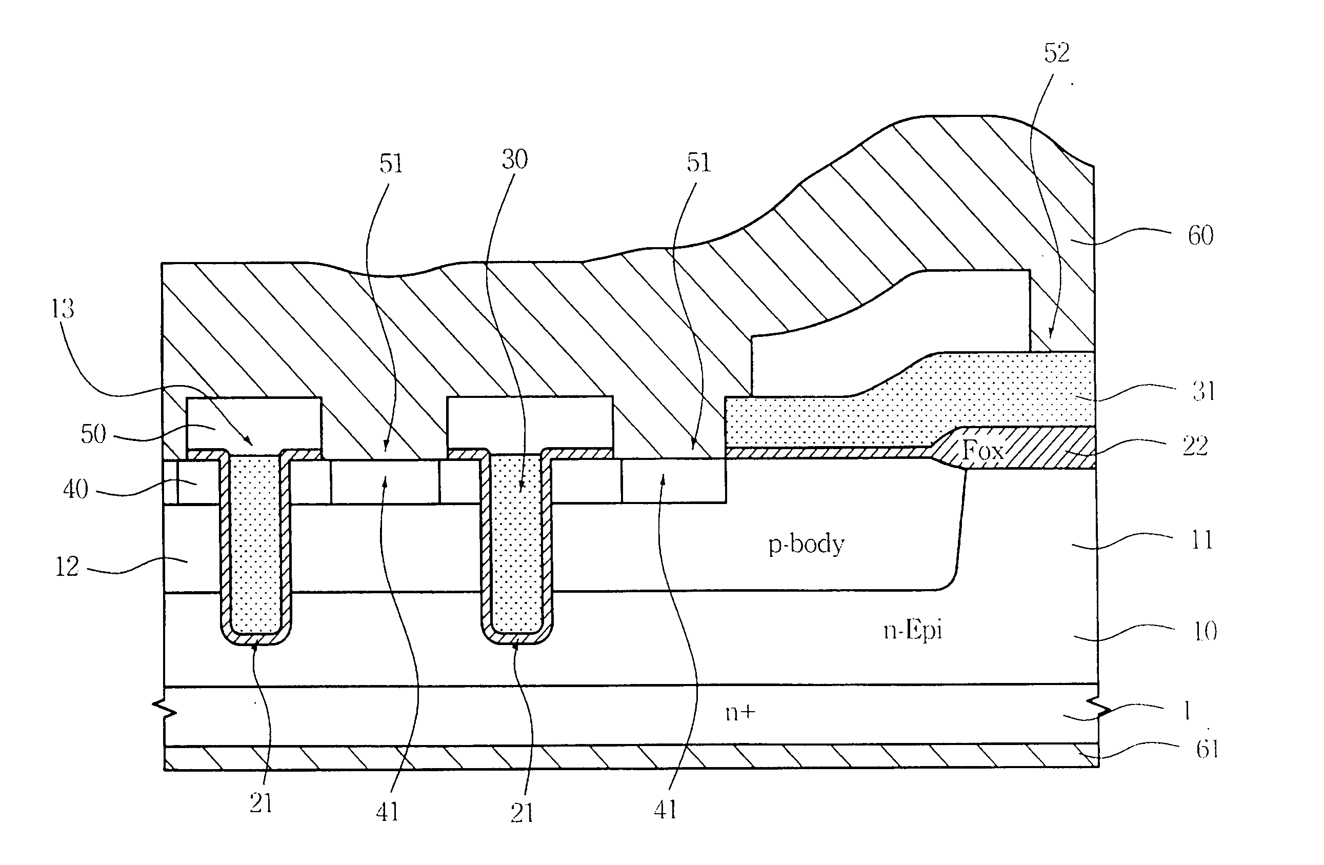
[0024] Embodiments of the invention disclosed herein are directed to a termination structure of DMOS device and a method for forming the same. In the following description, numerous details are set forth in order to provide a clear understanding of the present invention. It will be appreciated by one skilled in the art that variations of these specific details are possible while still achieving the results of the present invention. In some cases, well-known components are not described in detail in order not to unnecessarily obscure the present invention.
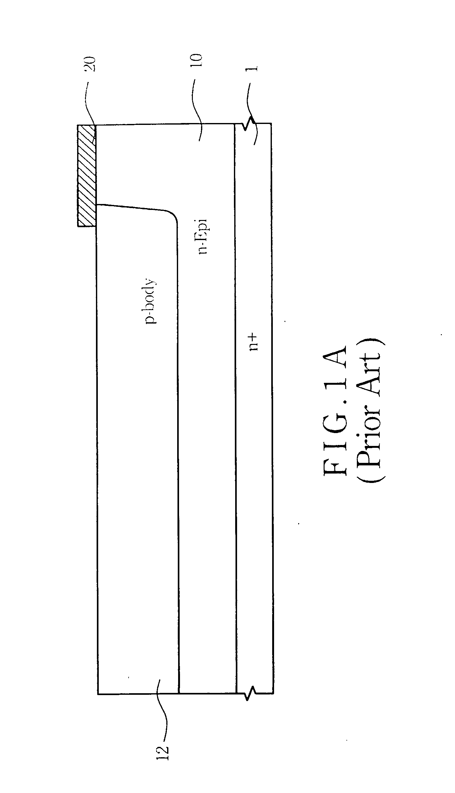
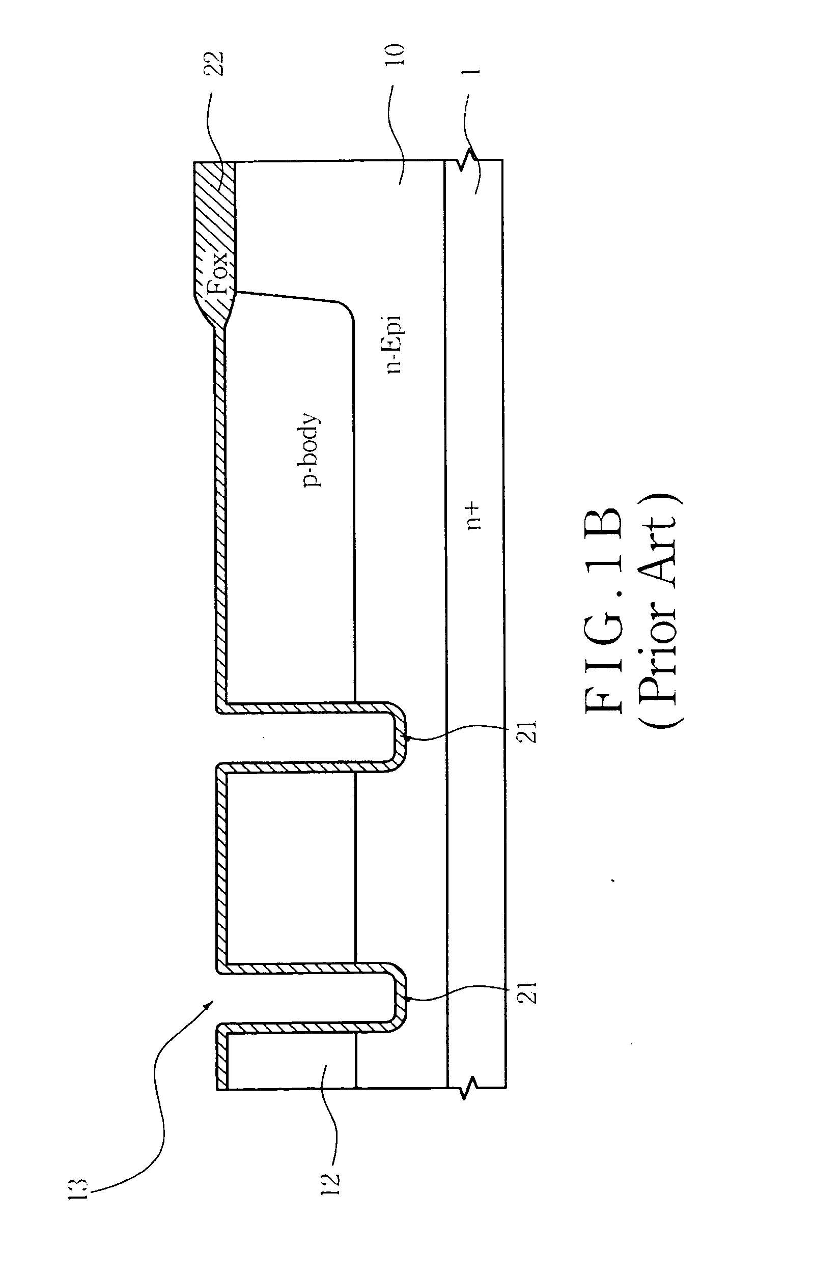
[0025] The fabrication processes of a trenched DMOS and a termination structure thereof in accordance with the present embodiment are shown in a schematic sequence of FIG. 5A through FIG. 5F.
[0026] As shown in FIG. 5A, an N-type epi layer 10 is formed on an N+-type silicon substrate 1. Afterward, an oxide layer is formed over the top surface of the N-type epi layer 10. A lithographic process is used to define an active area 12 and...
PUM
 Abstract
Description
Claims
Application Information
 - R&D
- Intellectual Property
- Life Sciences
- Materials
- Tech Scout
- Unparalleled Data Quality
- Higher Quality Content
- 60% Fewer Hallucinations
Browse by: Latest US Patents, China's latest patents, Technical Efficacy Thesaurus, Application Domain, Technology Topic, Popular Technical Reports.
© 2025 PatSnap. All rights reserved.Legal|Privacy policy|Modern Slavery Act Transparency Statement|Sitemap|About US| Contact US: help@patsnap.com


