Reworkable b-stageable adhesive and use in waferlevel underfill

Inactive Publication Date: 2004-06-10
GLOBALFOUNDRIES INC
View PDF4 Cites 48 Cited by
  • Summary
  • Abstract
  • Description
  • Claims
  • Application Information

AI Technical Summary

Problems solved by technology

However, since there is a significant mismatch of the coefficient of thermal expansion (CTE) between the chip silicon and the laminate material, DCA bonded chips must be underfilled with an adhesive support material; underfilling greatly increases the fatigue life of the solder bumps.
However, several manufacturing problems are associated with underfilling.
First, the process adds to the time required to bond each chip.
Upon completion of the underfill operation, batch curing is done requiring an additional amount of time.
Secondly, the distribution of the underfill may be incomplete since the conventional underfill process relies on capillary action to pull the liquid underfill completely under the chip.
Since it is difficult to determine underfill uniformity under the chip, partial fills occur which may lead to excess mechanical stress on affected bumps.
To avoid this problem, many flip chip packages are 100% inspected by scanning acoustic microscopy, an expensive and slow process.
Thirdly, underfilling adds cost since extra tooling, 0 line space and operator personnel are required.
Filled materials have been found not to work in no-flow applications due to the inclusion of particles in the solder joints which lead to electrically inferior and mechanically weak joints.
These application methods are deemed necessary to avoid inclusion of filler particles in the solder joint which is thought to increase electrical resistance and decrease mechanical integrity.
This same property of intractability of thermosets, however, is a liability since it prohibits rework or at least makes it very difficult.
If expensive chips or substrates are being used, the inability to rework is not acceptable since one defective part would render the whole assembly useless.
If a substrate holds more than one underfilled component as in high performance Multi Chip Modules (MCMs) and Flip-chip-on-Board (FCOB) applications, the inability to disassemble or "rework" a defective underfilled component can become very expensive since the whole package will become useless.
However, the site of the original, adhering, defective component, such as a flip chip, needs to be cleaned to receive a new, working component.
This site clean operation remains still the major roadblock to successful rework of thermoset underfilled chips.
This approach involves high temperature and harsh mechanical processes to clean the site.

Method used


Image

  • Reworkable b-stageable adhesive and use in waferlevel underfill
  • Reworkable b-stageable adhesive and use in waferlevel underfill
  • Reworkable b-stageable adhesive and use in waferlevel underfill

Examples


example 2

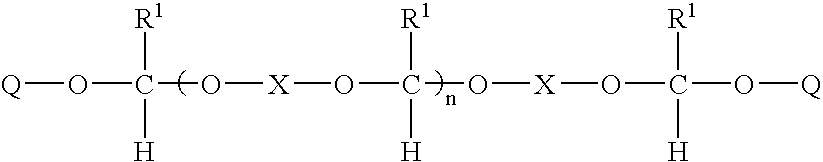
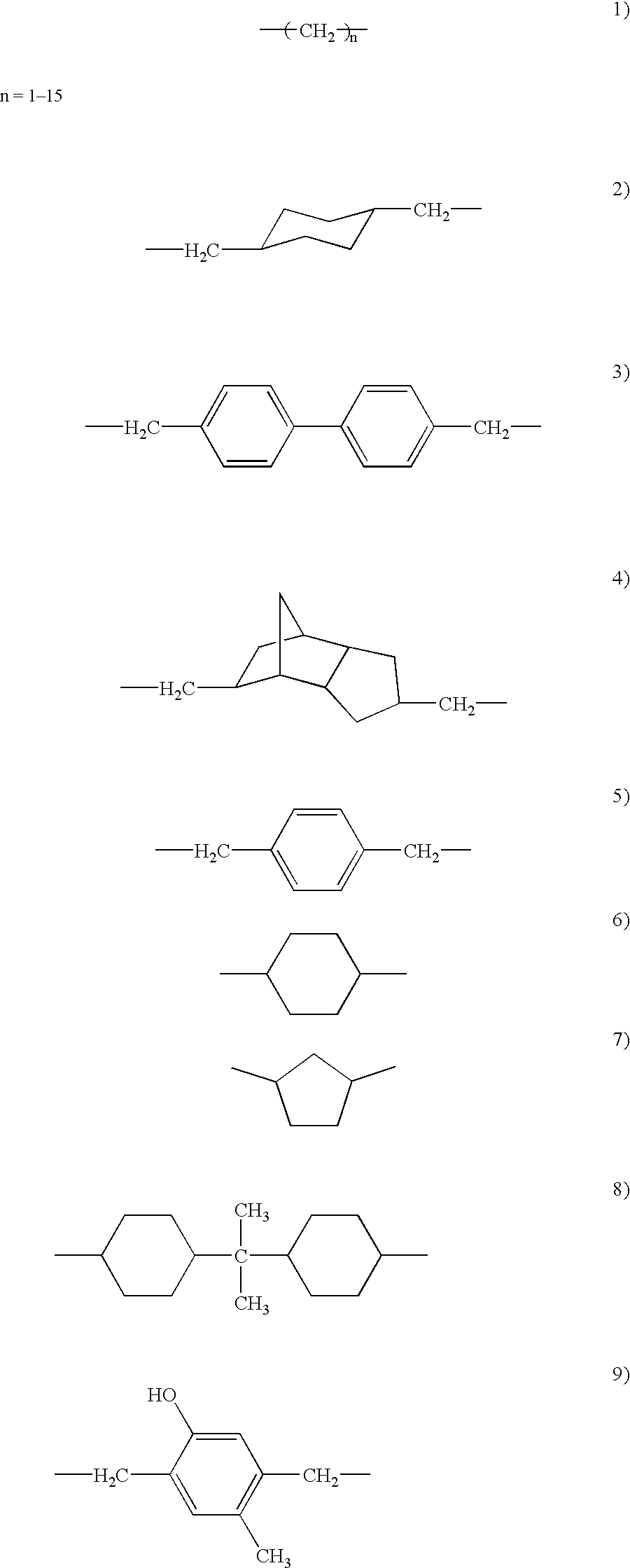
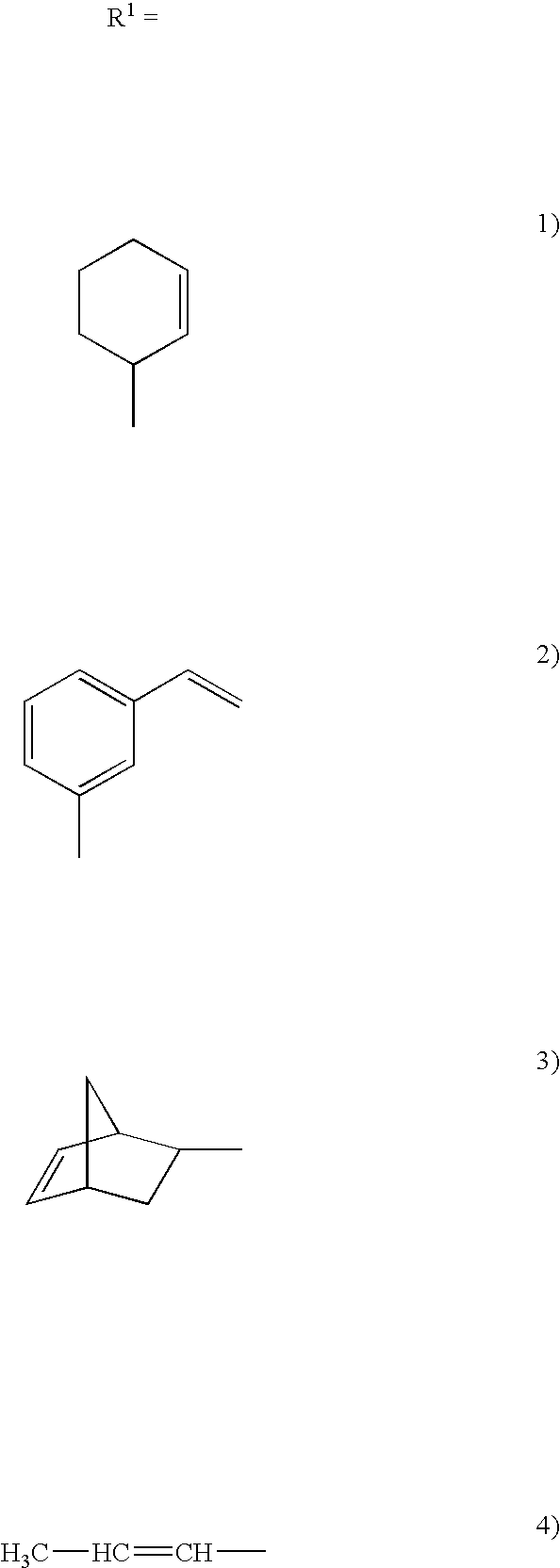
[0048] The schematic of the synthesis of a co-oligomer is shown in FIG. 3a. The synthesis of the co-oligomer was carried out similar to that of the oligomer discussed above. However, cyclohexane carboxaldehyde was used as a co-monomer. In the above scheme, the concentration of tetahydrobenzaldehyde to cyclohexane carboxaldehyde can be varied to tune the cured material properties. The monomer and co-monomer can also be changed. In general, the dialcohol and aldehydes can be changed in acetal oligomer synthesis as shown in FIG. 3b. The dialcohol can be aliphatic, aromatic or cyclic and aldehyde can be cyclic aliphatic or aromatic or any group illustrated in FIG. 3b. Unsaturated aldehyde can be used for epoxidation reaction. Aliphatic, aromatic or any other mono alcoholic group in FIG. 3b can be used for contolling the molecular weight of the oligomer.

example 3

[0049] Epoxidation of the acetal oligomer: The epoxidation was carried out by adopting the literature procedure (J. Rudolph, K. Laxma Reddy, J. P. Chiang, and K. Barry Sharpless J. Am. Chem. Soc. 119, 6189, 1997) as shown in FIG. 4a.

[0050] In a 250 ml three necked flask fitted with a mechanical stirrer, N.sub.2 inlet and outlet adapters, thermometer, and an addition funnel, 35 g (0.1494 mol) of acetal oligomer was dissolved in 200 ml of dichloromethane. To this, 1.45 ml of pyridine (0.01793 ml) and 0.1862 g (0.00075 mol) of methyl trioxorhenium was added as a catalyst. The reaction flask was cooled in an ice mixture. Exactly 25.6 ml (0.445 mol) of 50% hydrogen peroxide was added drop wise from an addition funnel so that the temperature of the reaction mixture did not raise to more than 5.degree. C. After completed addition, the reaction was allowed to continue to stir at room temperature for 24 hrs. After the reaction, the aqueous phase was separated and discarded. The remaining H.s...

example 4

[0051] Epoxidation of the acetal co-oligomer: The epoxidation was carried out using the same procedure which was used in Example 3.


PUM

PropertyMeasurementUnit
Fractionaaaaaaaaaa
Fractionaaaaaaaaaa
Fractionaaaaaaaaaa

Abstract

A reworkable thermoset epoxy-containing material that allows for a reworkable assembly such as a reworkable waferlevel underfilled miocroelectronic package. A method for using the reworkable thermoset material in the formation of a microelectronic package using this material.

Description

[0001] This invention relates to reworkable thermoset epoxy-containing material that allows for a reworkable assembly, for example a reworkable waferlevel underfilled microelectronic package. The invention also relates to a method using the reworkable thermoset matrial in the formation of a microelectronic package using this material, and other structures containing the reworkable thermoset epoxy-containing material.PRIOR ART[0002] Flip Chip technology has grown rapidly in recent years since it allows to decrease chip footprint while simultaneously increasing the number of possible I / O's. This is because flip chip technology takes advantage of the chip area for I / O's instead of just the chip periphery as in wire bonded chips. Various methods exist for solder bumping wafers, such as evaporation, plating, solder paste screening and more recently, injection molded solder, (IMS).[0003] Notwithstanding how the wafers are bumped, the bumped wafers typically are diced in the next step into...

Claims


Application Information

Patent Timeline
IPC IPC(8): C08G65/26H01L21/56H01L23/29
CPCC08G65/2654Y10T428/12528H01L23/293H01L2224/16225H01L2224/274H01L2224/73203H01L2224/73204H01L2224/83191H01L2224/83192H01L2924/01003H01L2924/01005H01L2924/01011H01L2924/01012H01L2924/01013H01L2924/01015H01L2924/01025H01L2924/01027H01L2924/01029H01L2924/0103H01L2924/01039H01L2924/01047H01L2924/01074H01L2924/01077H01L2924/01078H01L2924/01082H01L21/563H01L2924/10253H01L2924/01033H01L2924/01024H01L2924/01019H01L2924/01006H01L2224/32225H01L24/29H01L2924/00H01L2924/12042H01L2224/73104H01L2224/94H01L2924/00014Y10T428/31511H01L2224/27H01L2224/11H01L2224/0401
Inventor BUCHWALTER, STEPHEN LESLIEFEGER, CLAUDIUSHOUGHAM, GARETHLABIANCA, NANCYSHOBHA, HOSADURGA
Owner GLOBALFOUNDRIES INC
Why Eureka
Try Eureka