Solid state transmitter circuit
- Summary
- Abstract
- Description
- Claims
- Application Information
AI Technical Summary
Problems solved by technology
Method used
Image
Examples
Embodiment Construction
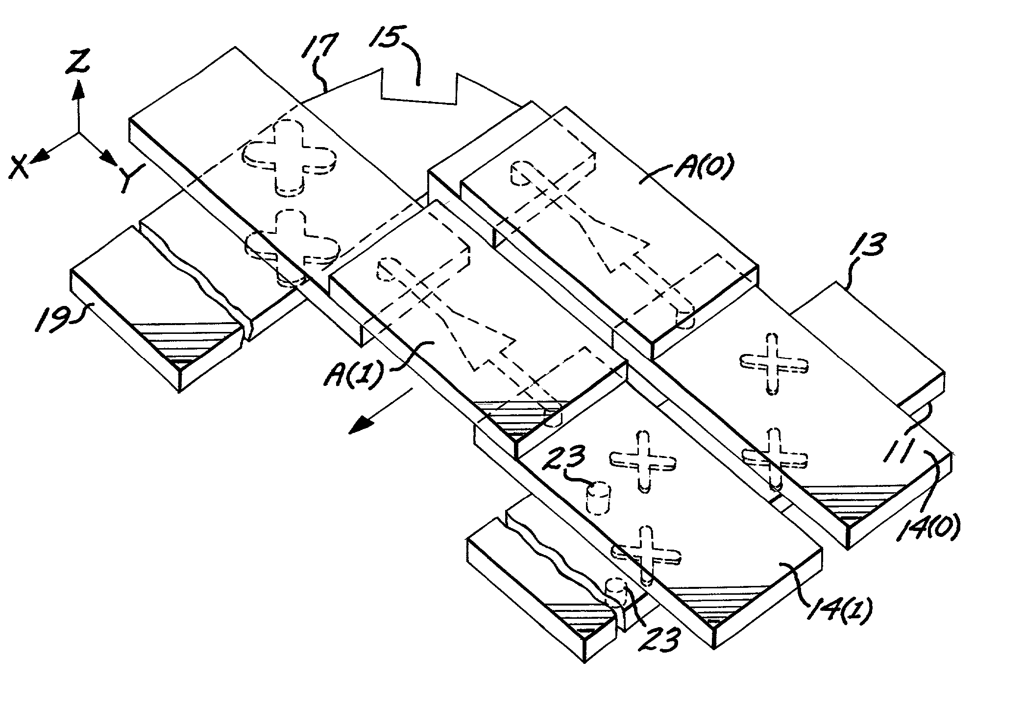
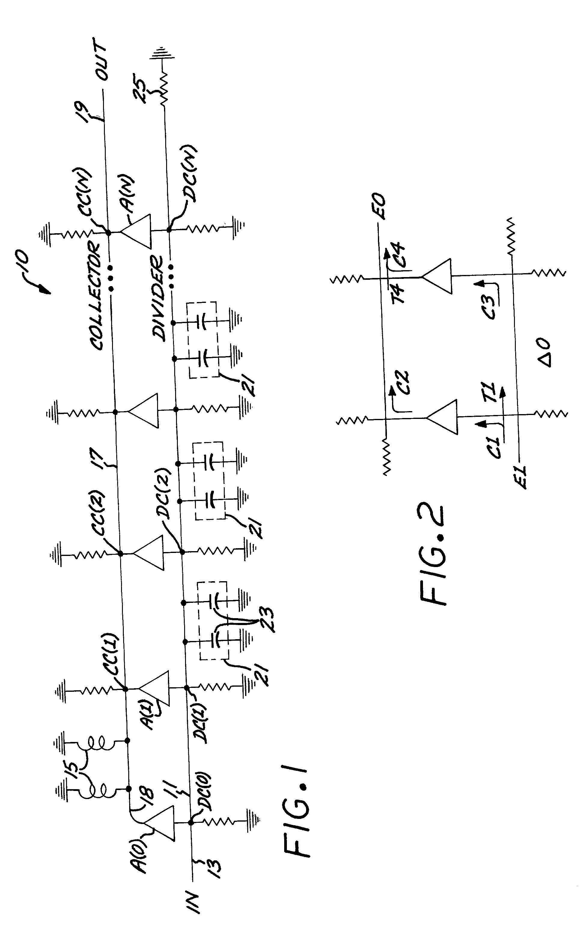
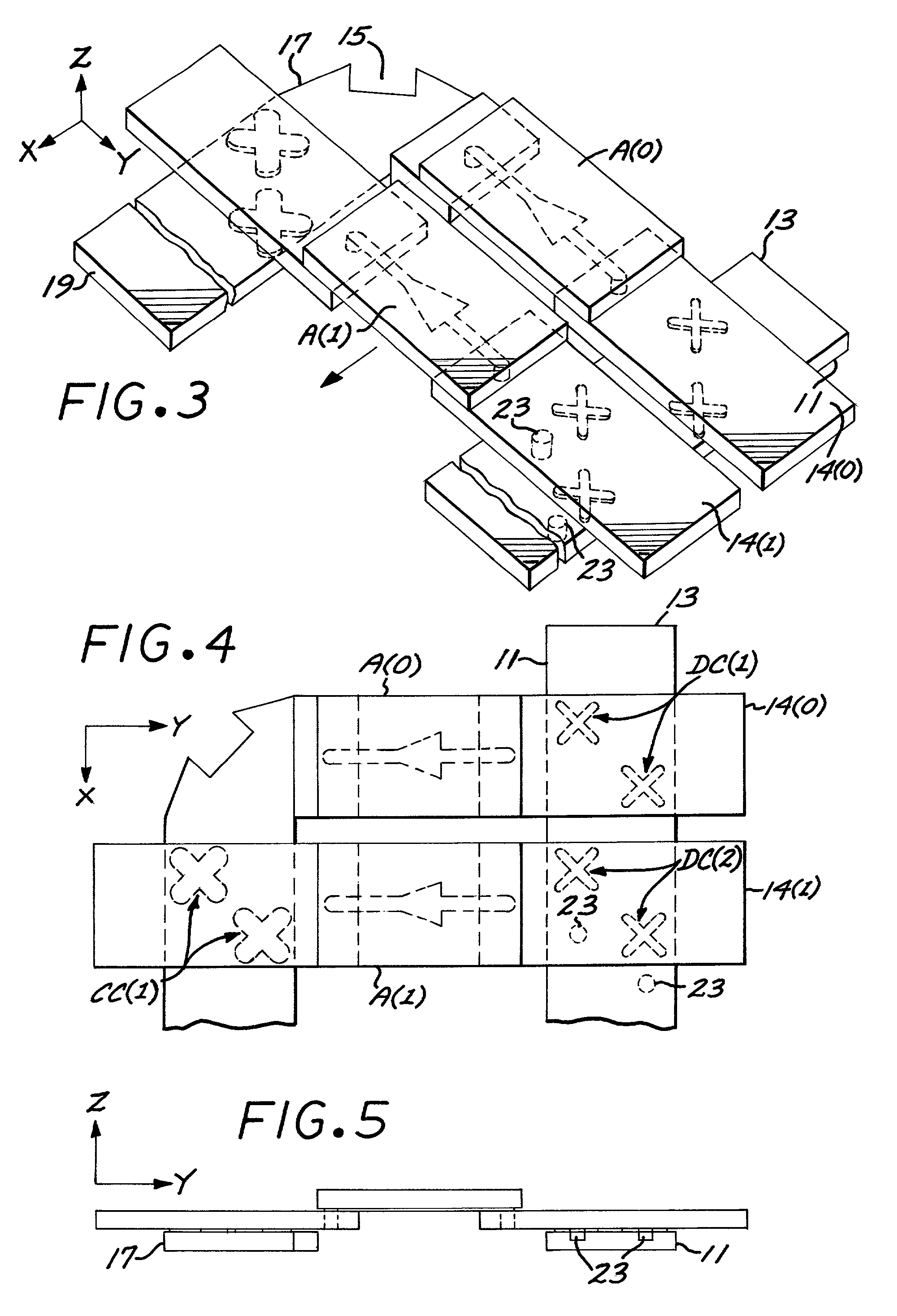
[0013] FIG. 1 is a schematic electrical diagram of elements of a solid state transmitter circuit 10 that employs features of the invention. The transmitter circuit 10 includes a divider series feed signal line or path 11 that receives an RF signal at an input or start 13 which is the input to the combiner circuit. The divider series feed signal path 11 can comprise a suitable microwave transmission line such as a waveguide. Respective divider directional couplers DC(0)-DC(N) are connected to the divider series feed signal line 11 at a spacing of about one half of a selected operational wavelength, typically for waveguide transmission lines, but not necessarily, particularly for applications using other transmission media, at the center of an operating frequency band. The 0.sup.th directional coupler DC(0) is located close to or at the input 13 of the divider feed line 11. The divider directional couplers DC(0)-DC(N) are configured to couple power from the divider feed line 11 to res...
PUM
 Abstract
Description
Claims
Application Information
 - R&D
- Intellectual Property
- Life Sciences
- Materials
- Tech Scout
- Unparalleled Data Quality
- Higher Quality Content
- 60% Fewer Hallucinations
Browse by: Latest US Patents, China's latest patents, Technical Efficacy Thesaurus, Application Domain, Technology Topic, Popular Technical Reports.
© 2025 PatSnap. All rights reserved.Legal|Privacy policy|Modern Slavery Act Transparency Statement|Sitemap|About US| Contact US: help@patsnap.com


