Bipolar transistor and method of manufacturing the same
a technology of bipolar transistor and manufacturing method, which is applied in the direction of transistors, electrical devices, semiconductor devices, etc., can solve the problems of difficult high frequency driving of bipolar transistors, and achieve the effect of improving the high frequency characteristics of bipolar transistors
- Summary
- Abstract
- Description
- Claims
- Application Information
AI Technical Summary
Benefits of technology
Problems solved by technology
Method used
Image

Examples
first embodiment
[0085] 1. First Embodiment
[0086] A. Structure
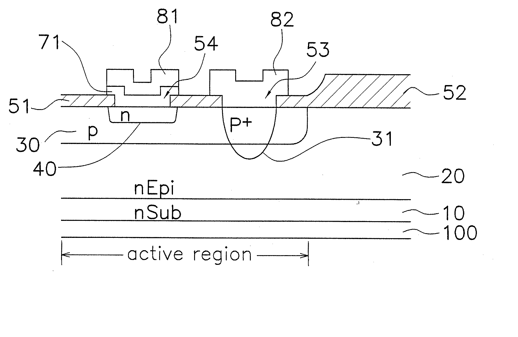
[0087] Fig. 1 is a cross-section of a bipolar transistor according to a first embodiment of the present invention. For the sake of simplicity, the same reference numerals used to describe the conventional bipolar transistor in Fig. 37 will be used in Figs. 1 to 8 when describing the same structures.
[0088] This bipolar transistor is comprised of an n-type semiconductor substrate 10, a collector region 20 that is formed on top of the n-type semiconductor substrate 10, a base region 30 that is formed inside the collector region 20, an emitter region 40 that is formed inside the base region 30, thermal oxide films 51, 52 that are formed on the surface of the base region 30 and the emitter region 40 and which include contact holes 53, 54, a base electrode 82 formed on top of the base region 30 through the contact hole 53, an emitter contact layer 71 composed of polysilicon and formed on top of the emitter region 40 through the contact hole 54,...
second embodiment
[0109] 2. Second Embodiment
[0110] A. Structure
[0111] Fig. 9 is a cross-section of a bipolar transistor according to a second embodiment of the present invention. For the sake of simplicity, the same reference numerals used to describe the conventional bipolar transistor in Fig. 37 will be used in Figs. 9 to 16 when describing the same structures.
[0112] This bipolar transistor is comprised of an n-type semiconductor substrate 10, a collector region 20 that is formed on top of the n-type semiconductor substrate 10, a base region 30 that is formed on the surface of the collector region 20, a base diffusion region 31 that is formed such that it lies on top of the base region 30, and an emitter region 40 that is formed inside the base region 30. In addition, a thermal oxide film 50 is formed on the surface of the base diffusion region 31 and the emitter region 40, and contact holes 91 and 92 are formed through the thermal oxide film 50 over the points where the base diffusion region 31 a...
third embodiment
[0126] 3. Third Embodiment
[0127] A. Structure
[0128] Fig. 19(a) is a plan view of a bipolar transistor according to a third embodiment of the present invention, Fig. 19(b) is a plan view of a diffusion region after the metal wiring shown in Fig. 19(a) is removed, and Fig. 19(c) is a cross-section of the interior of the semiconductor taken along the line A-A' in Fig. 19(a). For the sake of simplicity, the same reference numerals used to describe the bipolar transistor in the first embodiment will be used in Figs. 19 to 26 when describing the same structures.
[0129] As shown in Fig. 19(a), the bipolar transistor according to the third embodiment is formed such that the emitter electrode 81 and the emitter region 40, and the base electrode 82 and the base diffusion region 31, are sequentially disposed with respect to each other in a comb tooth like pattern. As shown in Fig. 19(c), collector wall regions 45 (n.sup.+ diffusion regions) are formed such that they surround the base region 30 ...
PUM
| Property | Measurement | Unit |
|---|---|---|
| thickness | aaaaa | aaaaa |
| thickness | aaaaa | aaaaa |
| thickness | aaaaa | aaaaa |
Abstract
Description
Claims
Application Information
 - R&D
- Intellectual Property
- Life Sciences
- Materials
- Tech Scout
- Unparalleled Data Quality
- Higher Quality Content
- 60% Fewer Hallucinations
Browse by: Latest US Patents, China's latest patents, Technical Efficacy Thesaurus, Application Domain, Technology Topic, Popular Technical Reports.
© 2025 PatSnap. All rights reserved.Legal|Privacy policy|Modern Slavery Act Transparency Statement|Sitemap|About US| Contact US: help@patsnap.com