Reconfigurable artificial magnetic conductor using voltage controlled capacitors with coplanar resistive biasing network
a voltage control capacitor and artificial magnetic conductor technology, applied in the direction of electrically short antennas, antenna feed intermediates, antennas, etc., can solve the problems of inefficient radiating and too large thickness for many practical applications
- Summary
- Abstract
- Description
- Claims
- Application Information
AI Technical Summary
Problems solved by technology
Method used
Image
Examples
second embodiment
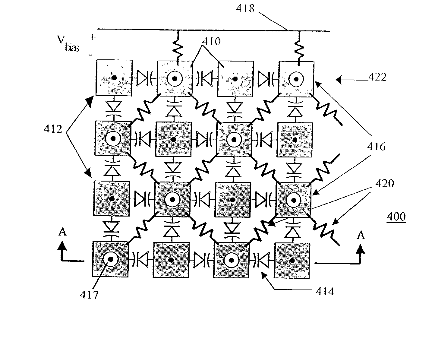
[0054] FIG. 6 is a top view and FIG. 7 is a cross sectional view of a reconfigurable artificial magnetic conductor (RAMC) 400. This embodiment is a "thinned" version of the embodiment shown in FIGS. 4 and 5. The RAMC 400 includes a frequency selective surface (FSS) 402, a spacer layer 404 penetrated by conducting vias 408 and a backplane or ground plane 406. The vias are in electrical contact with the ground plane 406, which is typically kept at ground potential or other reference voltage.
[0055] The FSS 402 includes an array of conductive patches 410. Each patch 410 is associated with a via 408 of the spacer layer. Each patch 410 of a first group 412 of patches 410 is electrically coupled with its associated via so that the patch is maintained at ground or other reference potential. Each patch 410 of a second group 416 is not electrically coupled with its associated via but is electrically isolated from the grounded via 408. The patches 410 in the illustrated embodiment are arranged...
sixth embodiment
[0070] FIG. 16 is a cross sectional view of a reconfigurable artificial magnetic conductor (RAMC) 1600. The RAMC 1600 includes a frequency selective surface (FSS) 1602, a dielectric spacer layer 1604, a backplane or ground plane 1606, and conductive vias 1608 extending from the ground plane 1606 through the spacer layer 1604 to form a rodded medium.
[0071] The FSS 1602 includes a tunable dielectric film 1614, which may be a ferroelectric material such as Barium Strontium Titanate Oxide (BSTO), a first layer 1610 of conductive patches on one side of the tunable dielectric film 1614 and a second layer 1612 of conductive patches on a second side of the tunable dielectric film. The patches of the second layer 1612 overlap at least in part patches of the first layer 1610. The vias 1608 include first vias 1618 associated with patches of the first layer 1610 and second vias 1616 associated with patches of the second layer 1612. The backplane 1606 includes a stripline bias distribution layer...
PUM
 Abstract
Description
Claims
Application Information
 - R&D
- Intellectual Property
- Life Sciences
- Materials
- Tech Scout
- Unparalleled Data Quality
- Higher Quality Content
- 60% Fewer Hallucinations
Browse by: Latest US Patents, China's latest patents, Technical Efficacy Thesaurus, Application Domain, Technology Topic, Popular Technical Reports.
© 2025 PatSnap. All rights reserved.Legal|Privacy policy|Modern Slavery Act Transparency Statement|Sitemap|About US| Contact US: help@patsnap.com


