Transparent electrode for optoelectronic components

a technology of transparent electrodes and optoelectronic components, which is applied in the direction of sustainable manufacturing/processing, sustainable building construction, and final product manufacturing, etc., can solve the problems of inability to use monocrystalline organic materials, inability to produce multiple layers with sufficient structural perfection, and inability to meet the requirements of the production process

Active Publication Date: 2022-06-07
HELIATEK GMBH
View PDF44 Cites 0 Cited by
  • Summary
  • Abstract
  • Description
  • Claims
  • Application Information

AI Technical Summary

Problems solved by technology

These thin-film solar cells have the disadvantage above all of the high production costs due to the materials.
However, for large-area applications, the use of monocrystalline organic materials is not possible and the production of multiple layers with sufficient structural perfection is still very difficult up to this point.
The top contacts previously described in the

Method used


Image

  • Transparent electrode for optoelectronic components
  • Transparent electrode for optoelectronic components

Examples


Embodiment Construction

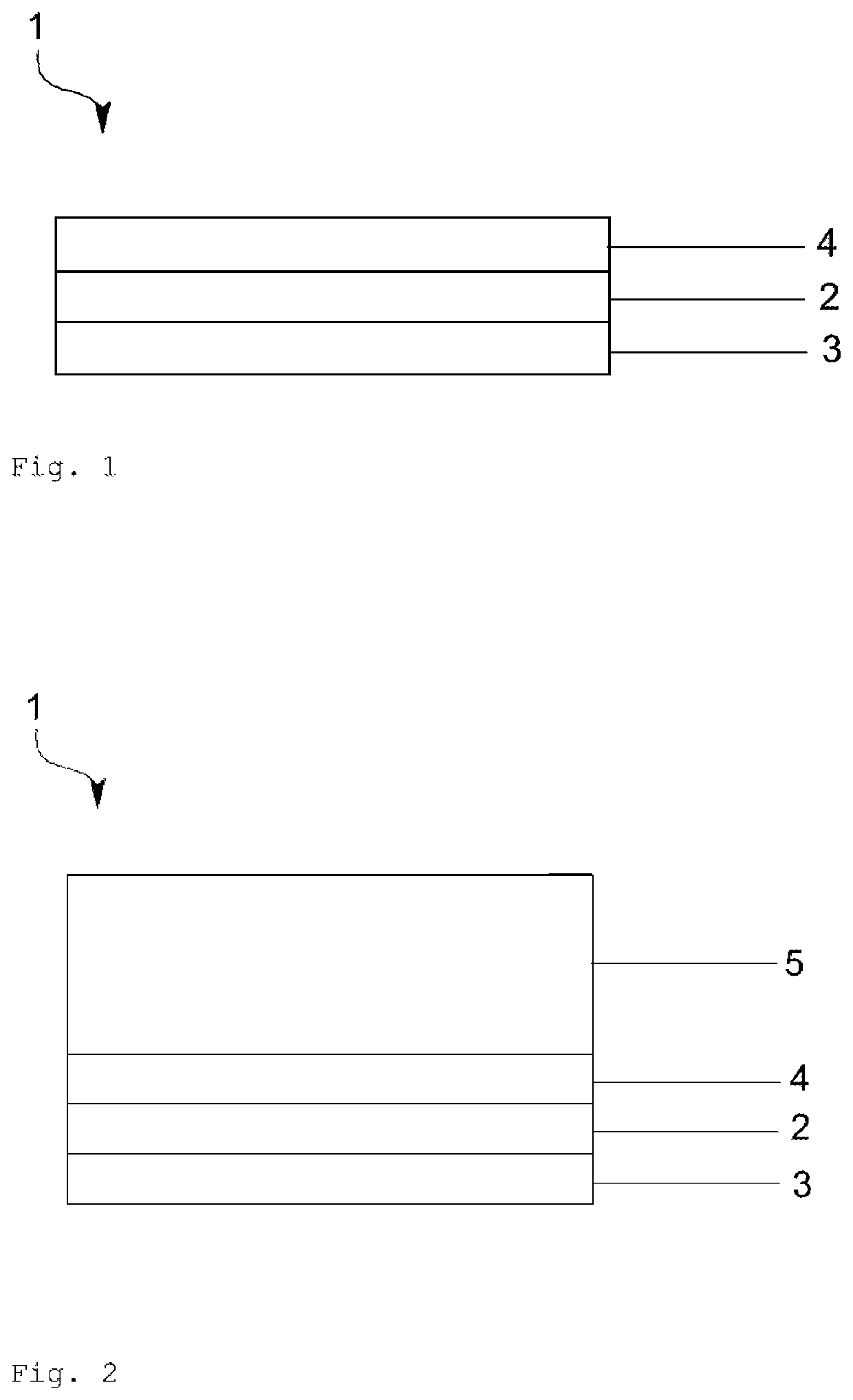
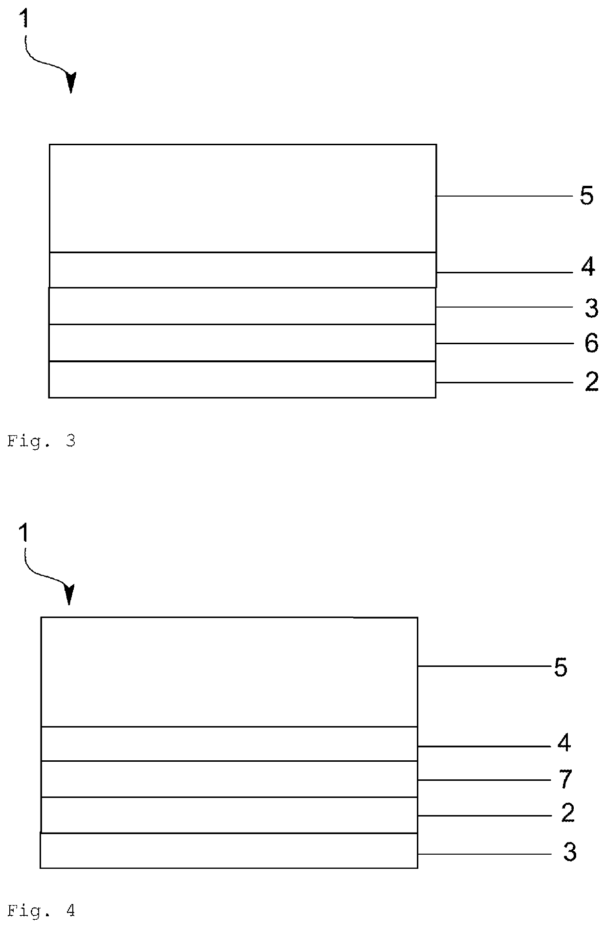
[0127]In one exemplary embodiment of the invention, an electrode arrangement 1 according to the invention is shown in FIG. 1, which comprises a first intermediate layer 3 made of a metal or metal oxide, for example, made of MoO3. The first intermediate layer 3 is deposited in this case by thermal vapor deposition on an organic layer of the component. A first layer 2 comprising a metal, for example, Ag, is deposited thereon. The deposition is performed in this case by means of sputtering. A second layer 4 is arranged as an antireflection layer, which comprises, for example, N,N′-bis(naphthalene-1-yl)-N,N′-bis(phenyl)-benzidine, on this first layer 2.

[0128]In a further exemplary embodiment of the invention (not shown in greater detail), the electrode arrangement 1 according to the invention comprises a first intermediate layer 3 made of a metal or metal oxide, for example, made of MoO3. The first intermediate layer 3 is deposited in this case by thermal vapor deposition on an organic ...


PUM


Abstract

An optoelectronic component on a substrate includes a first and a second electrode. The first electrode is arranged on the substrate and the second electrode forms a counter electrode. At least one photoactive layer system is arranged between these electrodes. The at least one photoactive layer system including at least one donor-acceptor system having organic materials.

Description

CROSS REFERENCE TO RELATED APPLICATIONS[0001]This application is a national stage filing under section 371 of International Application No. PCT / IB2013 / 055425, filed on Jul. 2, 2013, and published in German on Jan. 9, 2014 as WO 2014 / 006565 A2, which claims priority to German Application No. 102012105809.1, filed on Jul. 2, 2012, and German Application No. 102012105810.5, filed on Jul. 2, 2012, the entire content of said applications being hereby incorporated herein by reference.BACKGROUND ART[0002]The invention relates to a transparent electrode for optoelectronic components.[0003]Optoelectronic components, for example, solar cells or LEDs, TFTs, etc., currently have broad applications in the everyday environment and the industrial environment. In this case, those components which enable an arrangement on curved or bulging surfaces because of their embodiment are of particular interest.[0004]Thus, for example, thin-film solar cells are known, which have a flexible design and therefo...

Claims


Application Information

Patent Timeline
IPC IPC(8): H01L51/44H01L51/00H01L51/42H01L51/52
CPCH01L51/442H01L51/0021H01L51/4293H01L51/5231Y02B10/10Y02E10/549Y02P70/50H10K30/82H10K71/60H10K30/40H10K50/826H01L2031/0344
Inventor PFEIFFER, MARTINUHRICH, CHRISTIANBEWERSDORFF-SARLETTE, ULRIKEMEISS, JANLEO, KARLRIEDE, MORITZSCHUBERT, SYLVIOMUELLER-MESKAMP, LARS
Owner HELIATEK GMBH
Why Eureka
Try Eureka