Semiconductor device, layout design method for the same and method for fabricating the same

a semiconductor device and layout design technology, applied in computer aided design, instruments, nanoinformatics, etc., can solve the problems of complex structure and high integration of semiconductor devices, and achieve the effects of reducing power loss and resource loss of pnr (placement and routing) and reducing the use of top wirings

Active Publication Date: 2022-06-07
SAMSUNG ELECTRONICS CO LTD
View PDF8 Cites 0 Cited by
  • Summary
  • Abstract
  • Description
  • Claims
  • Application Information

AI Technical Summary

Benefits of technology

[0005]Aspects of inventive concepts provide a semiconductor device in which the use of top wirings is reduced and power loss and PnR (Placement and Routing) resource loss is reduced.
[0006]Aspects of inventive concepts also provide a layout design method for a semiconductor device in which the use of top wirings is reduced and power loss and PnR resource loss are reduced.
[0007]Aspects of inventive concepts also provide a method for fabricating a semiconductor device in which the use of top wirings is reduced and the power loss and the PnR resource loss are reduced.

Problems solved by technology

In order to satisfy these desired characteristics, the structure in the semiconductor device becomes increasingly complicated and highly integrated.

Method used


Image

  • Semiconductor device, layout design method for the same and method for fabricating the same
  • Semiconductor device, layout design method for the same and method for fabricating the same
  • Semiconductor device, layout design method for the same and method for fabricating the same

Examples


Embodiment Construction

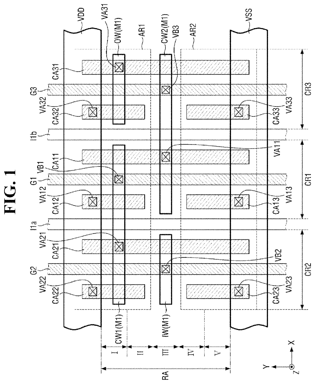
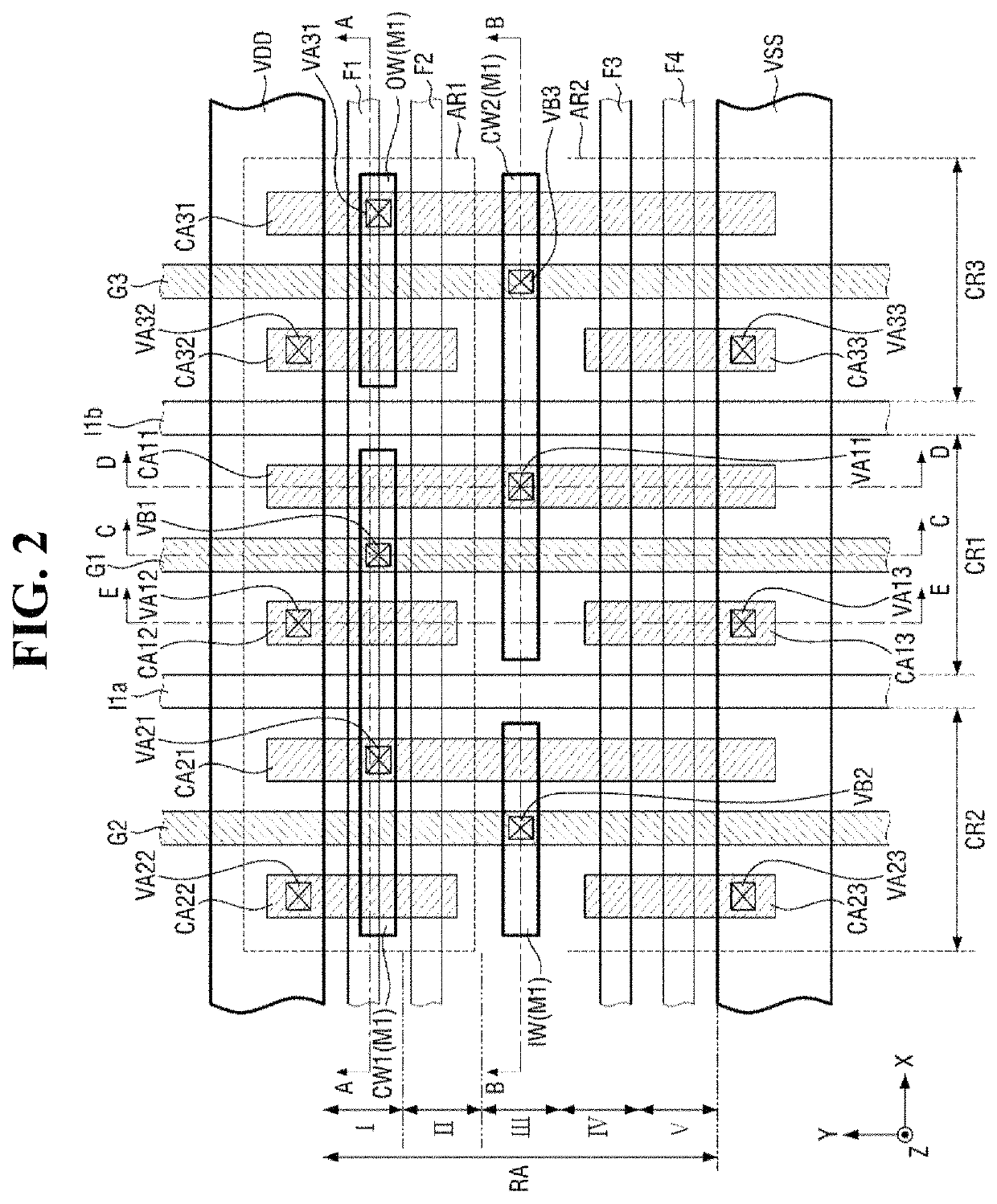
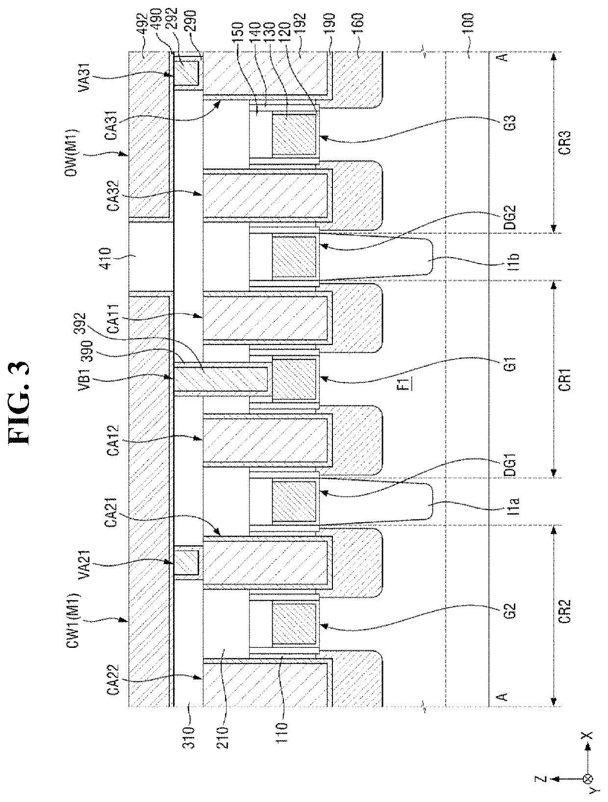
[0029]Hereinafter, a semiconductor device according to some embodiments will be described with reference to FIGS. 1 through 18.

[0030]In the drawings of the semiconductor device according to some embodiments, although a fin-type transistor (FinFET) including a channel area having a fin-type pattern shape is shown as examples, the present disclosure is not limited thereto. The semiconductor device according to some embodiments may, of course, include a tunneling transistor (FET), a transistor including a nanowire, a transistor including a nanosheet or a three-dimensional (3D) transistor. Also, the semiconductor device according to some embodiments of inventive concepts may include a bipolar junction transistor, a lateral double diffusion transistor (LDMOS), and the like.

[0031]It will be understood that, although the terms first, second, etc. may be used herein to describe various elements, these elements should not be limited by these terms. These terms are only used to distinguish on...


PUM

PropertyMeasurementUnit
drain voltageaaaaaaaaaa
source voltageaaaaaaaaaa
speedaaaaaaaaaa

Abstract

A semiconductor device includes a first and second active pattern extending in a first direction on a substrate, a first and second gate electrode extending in a second direction to intersect the first and second active pattern, a first source / drain contact extending in the second direction and connected to a first and source / drain region of the first and second active patterns, respectively, a first source / drain via connected to the first source / drain contact, a first cell separation film extending in the second direction and crosses the first active pattern and the second active pattern, between the first source / drain contact and the second gate electrode, a first gate via connected to the second gate electrode and arranged with the first source / drain via along the first direction, and a first connection wiring which extending in the first direction and connects the first source / drain via and the first gate via.

Description

[0001]This application claims priority to Korean Patent Application No. 10-2019-0124324, filed on Oct. 8, 2019, and all the benefits accruing therefrom under 35 U.S.C. § 119, the disclosure of which is incorporated herein by reference in its entirety.BACKGROUND1. Technical Field[0002]Inventive concepts relate to a semiconductor device, a layout design method for the semiconductor device, and a method for fabricating the semiconductor device.2. Description of Related Art[0003]Due to characteristics such as miniaturization, multi-functionality and / or low fabricating cost, semiconductor devices are in the limelight as important elements in the electronics industry. Semiconductor devices may be classified into a semiconductor memory device that stores logic data, a semiconductor logic device that performs arithmetic processing on the logic data, and a hybrid semiconductor device including a memory element and a logic element and the like.[0004]As the electronics industry is highly devel...

Claims


Application Information

Patent Timeline
Patent Type & Authority Patents(United States)
IPC IPC(8): H01L29/417H01L27/088H01L29/40H01L29/78H01L23/522G06F30/392G06F30/3953H01L29/423H01L29/66H01L23/528G06F119/06
CPCH01L29/41791G06F30/392G06F30/3953H01L23/528H01L23/5226H01L27/0886H01L29/401H01L29/42372H01L29/66795H01L29/785G06F2119/06H01L27/0207H01L27/092H01L29/775H01L21/823431H01L29/78696H01L29/42392B82Y10/00H01L29/0673H01L23/5286H01L23/485H01L21/76895H01L27/0218H01L27/0611H01L29/41725H01L29/0653
Inventor YU, JI SUYOU, HYEON GYULIM, SEUNG MAN
Owner SAMSUNG ELECTRONICS CO LTD
Why Eureka
Try Eureka