Power converter module

a power converter module and module technology, applied in the direction of cross-talk/noise/interference reduction, inductance with magnetic core, inductance, etc., can solve the problems of increasing the proportion of this loss in the total loss of the power converter module, reducing and increasing the ac loss. , to achieve the effect of reducing the parasitic loss, and improving the conversion efficiency of the power conversion modul

Active Publication Date: 2022-02-15
DELTA ELECTRONICS INC
View PDF8 Cites 0 Cited by
  • Summary
  • Abstract
  • Description
  • Claims
  • Application Information

AI Technical Summary

Benefits of technology

The present disclosure provides a power converter module that improves conversion efficiency by reducing parasitic inductance and loss through the staggering of multiple copper layers and capacitors. The module has multiple positive and negative copper layers connected to terminals and vias, with projections of the layers partially overlapping on the first surface. This reduces the inductance and loss of the wiring, leading to improved power conversion.

Problems solved by technology

As the output power of the existing power converter module increases, the large current in the power converter module causes more and more losses in the corresponding current loop and flow path, and the proportion of this loss in the total loss of the power converter module also increases.
However, due to the existence of parasitic parameters between multiple copper layers and the AC loop in the power converter module.
This increases the AC loss of the AC current in the corresponding AC circuit, thereby reducing the conversion efficiency of the power conversion module.

Method used


Image

  • Power converter module
  • Power converter module
  • Power converter module

Examples


Embodiment Construction

[0016]The present disclosure will now be described more specifically with reference to the following embodiments. It is to be noted that the following descriptions of preferred embodiments of this disclosure are presented herein for purpose of illustration and description only. It is not intended to be exhaustive or to be limited to the precise form disclosed.

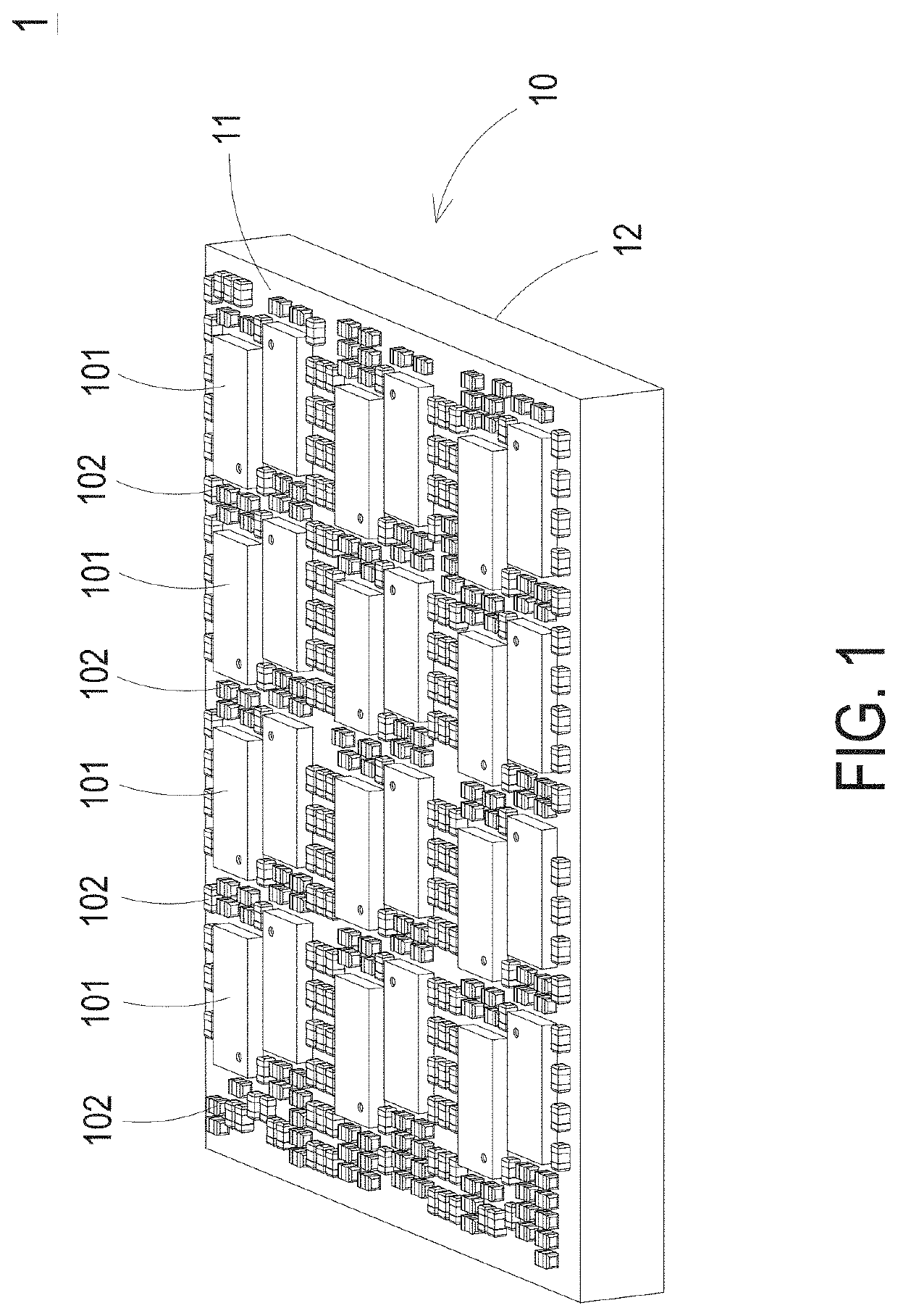
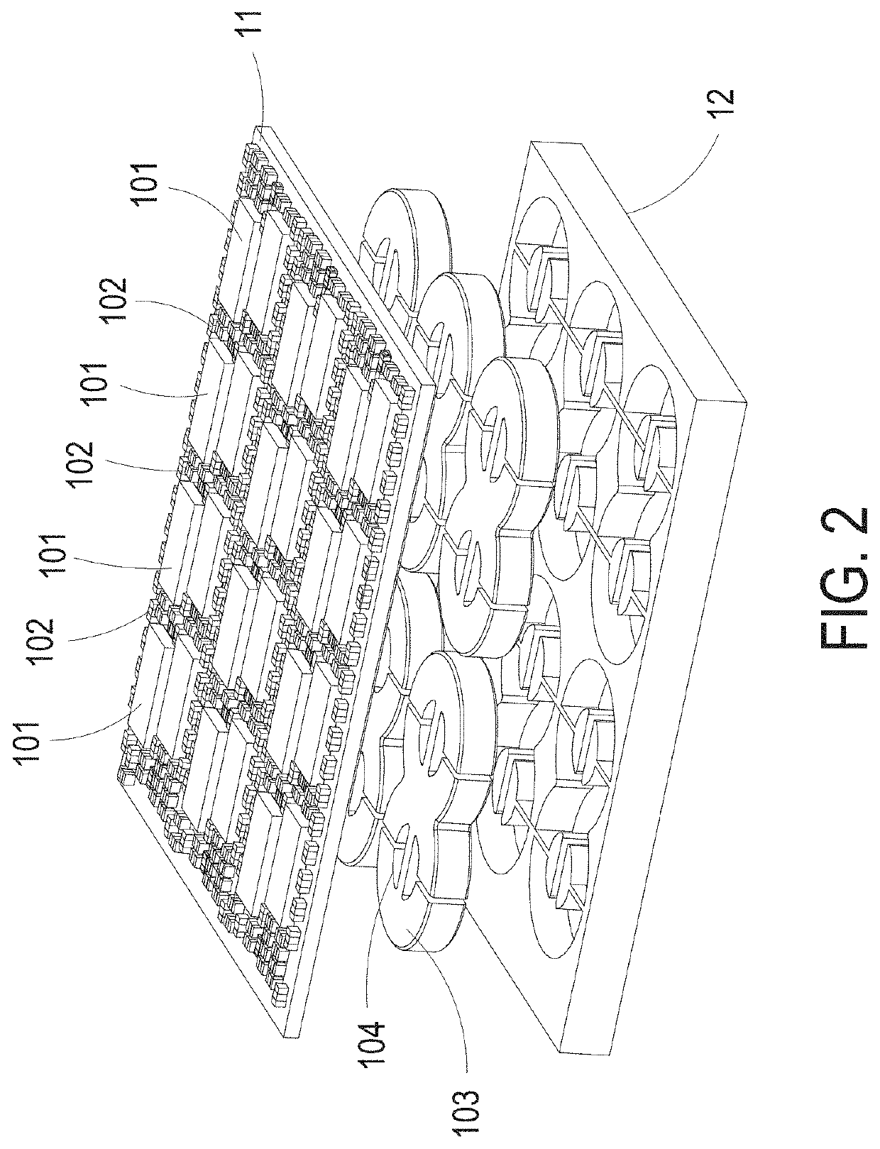
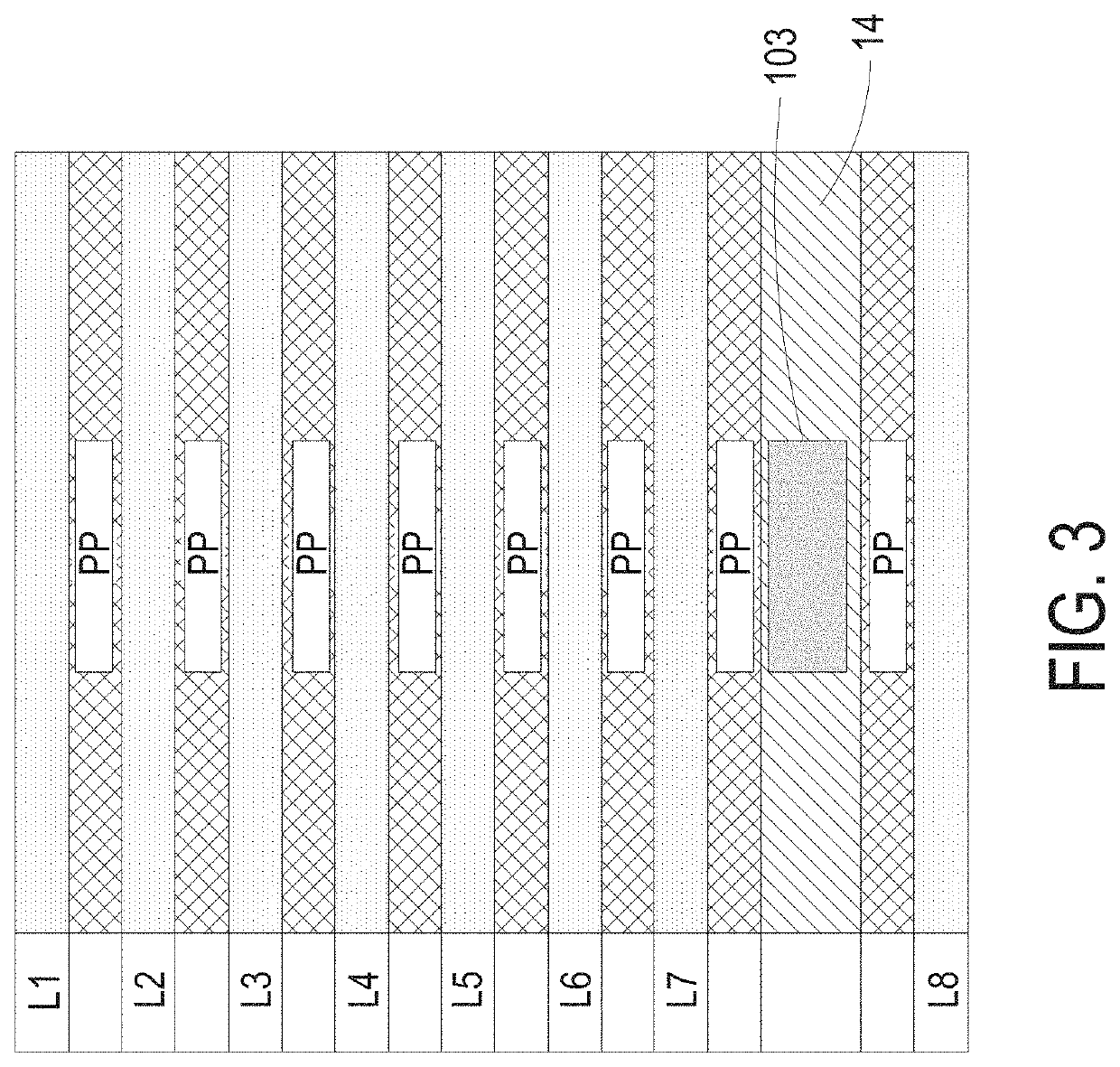
[0017]FIG. 1 is a schematic perspective view illustrating a power converter module according to an embodiment of the present disclosure. FIG. 2 is an exploded view illustrating the power converter module according to the embodiment of the present disclosure. FIG. 3 is a schematic side view illustrating the power converter module according to the embodiment of the present disclosure. FIG. 4 is a schematic side view illustrating the power converter module according to the embodiment of the present disclosure. As shown in FIGS. 1, 2, 3, and 4, the power converter module 1 includes a multilayer printed circuit board 10, at least on...


PUM

PropertyMeasurementUnit
areaaaaaaaaaaa
power poweraaaaaaaaaa
sizeaaaaaaaaaa

Abstract

A power converter module includes a multilayer printed circuit board, a switching device, a capacitor device, a first via, a second via, a third via and a fourth via. The multilayer printed circuit board has a first surface and a second surface and includes a plurality of copper layers including a plurality of positive copper layers and negative copper layers. The plurality of positive copper layers and the negative copper layers are disposed in staggered arrangement. The switching device is disposed on the first surface and includes a switching positive terminal and a switching negative terminal. The capacitor device is disposed on the first surface and includes a capacitor positive terminal and a capacitor negative terminal, and the capacitor device forms a capacitor area. The projections of the adjacent positive and negative copper layers and the capacitor area on the first surface at least partially overlap with each other.

Description

CROSS-REFERENCE TO RELATED APPLICATION[0001]This application claims priorities to China Patent Application No. 202011164463.3 filed on Oct. 27, 2020, and China Patent Application No. 202011239669.8 filed on Nov. 9, 2020, the entire content of which is incorporated herein by reference for all purposes.FIELD OF THE INVENTION[0002]The present disclosure relates to a power converter module, and more particularly to a power converter module with a plurality of positive copper layers and a plurality of negative copper layers staggered.BACKGROUND OF THE INVENTION[0003]With the rapid development of technologies such as mobile communications and cloud computing, high-power power converter modules have been widely used in electronic products. Due to the trend of high power and miniaturization of electronic products, how to improve the conversion efficiency of the power converter module and reduce the size of the power converter module is the primary consideration.[0004]As the output power of ...

Claims


Application Information

Patent Timeline
Patent Type & Authority Patents(United States)
IPC IPC(8): H05K1/16H05K1/11
CPCH05K1/165H05K1/115H05K2201/10015H05K2201/10053H05K2201/0792H05K2201/09309H05K2201/10166H05K1/0243H05K1/0231H05K2201/086H01F17/0013H01F17/04
Inventor JIN, DACUI, JUNGUOCHENG, CHENGLU, SHENGLI
Owner DELTA ELECTRONICS INC
Why Eureka
Try Eureka