Substrate holding member
a technology of holding member and substrate, which is applied in the direction of semiconductor/solid-state device manufacturing, basic electric elements, electrical equipment, etc., can solve the problems of peeling or cracking between the base and the protection film during long-term use, difficult to hold the substrate with a satisfactory flatness, peeling or cracking, etc., to inhibit the peeling of the holding member from the base
- Summary
- Abstract
- Description
- Claims
- Application Information
AI Technical Summary
Benefits of technology
Problems solved by technology
Method used
Image
Examples
first embodiment
[0036]A substrate holding member 1 according to the present invention will be described with reference to the drawings.
[0037]As shown in a cross-sectional view of FIG. 1, the substrate holding member 1 includes: a disk-shaped base 10; and a plurality of convex parts (projecting portions, pins) 20 which are formed on an upper surface of the base 10, and hold a wafer (substrate), which is not shown, at top surfaces 20a thereof.
[0038]In the substrate holding member 1, as shown in a partially enlarged cross-sectional view of FIG. 2, each convex part 20 has: a root portion 21 extending from the upper surface of the base 10; and a top portion 22 formed on the root portion 21 and including the top surface 20a. In the convex part 20, a cross-sectional area S1 of the root portion 21 in a horizontal direction (right-left direction in FIG. 2) along the upper surface of the base 10 is larger than a cross-sectional area S2 of the top portion 22 in the horizontal direction.
[0039]At least a portio...
second embodiment
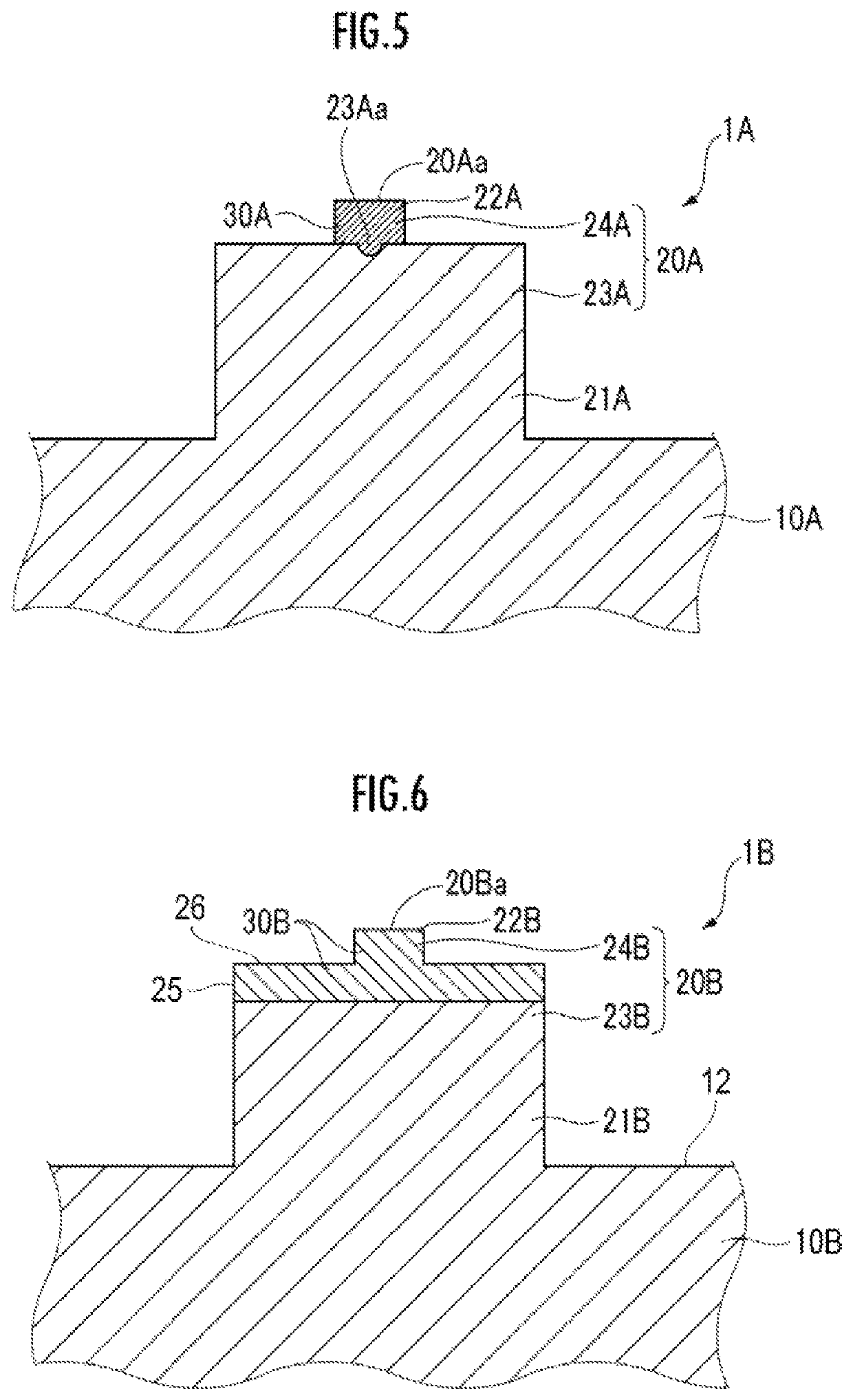
[0064]Next, a substrate holding member 1A according the present invention will be described with reference to the drawing. As shown in FIG. 5, the substrate holding member 1A is different from the aforementioned substrate holding member 1 only in that a holding member 30A is formed also in a recess 23Aa formed at an upper surface of a lower part 23A.
[0065]Thus, the holding member 30A is formed in such a shape that a portion thereof formed in the recess 23Aa of the lower part 23A and the entirety of an upper part 24A are integrated with each other. A cross-sectional shape of the recess 23Aa in the vertical direction is not particularly limited, and may be a semi-circle, a semi-ellipse, a rectangle, or the like, or may be such a shape that an inner portion thereof laterally expands as compared with an opening thereof. The recess 23Aa preferably has a depth of 0.01 to 0.2 mm, and an opening width of 0.02 to 0.2 mm.
[0066]The holding member 30A may be formed as follows. That is, after th...
third embodiment
[0069]Next, a substrate holding member 1B according to the present invention will be described with reference to the drawing. As shown in FIG. 6, the substrate holding member 1B is different from the aforementioned substrate holding member 1 only in that an upper portion of a lower part 23B is made of the same material as an upper part 24B forming a portion of the holding member 30B.
[0070]Thus, the holding member 30B is formed in such a shape that the upper portion of the lower part 23B and the entirety of the upper part 24B are integrated with each other. A lower portion of the lower part 23B is formed continuously from the base 10. In other words, the lower portion of the lower part 23B extends from the upper surface 12 of the base 10. The thickness of the holding member 30B at the upper portion of the lower part 23B is preferably 0.01 to 0.2 mm.
[0071]According to the substrate holding member1B described above, like the aforementioned substrate holding member 1, the wafer can be h...
PUM
 Abstract
Description
Claims
Application Information
 - R&D
- Intellectual Property
- Life Sciences
- Materials
- Tech Scout
- Unparalleled Data Quality
- Higher Quality Content
- 60% Fewer Hallucinations
Browse by: Latest US Patents, China's latest patents, Technical Efficacy Thesaurus, Application Domain, Technology Topic, Popular Technical Reports.
© 2025 PatSnap. All rights reserved.Legal|Privacy policy|Modern Slavery Act Transparency Statement|Sitemap|About US| Contact US: help@patsnap.com


