Solid-state imaging apparatus, method for manufacturing the same, and electronic device
a technology of solid-state imaging and manufacturing methods, applied in the direction of radio frequency controlled devices, instruments, television systems, etc., can solve the problems of color separation and s/n deterioration, and achieve the effect of suppressing the occurrence of color mixing between pixels
- Summary
- Abstract
- Description
- Claims
- Application Information
AI Technical Summary
Benefits of technology
Problems solved by technology
Method used
Image
Examples
first embodiment
3. First Embodiment
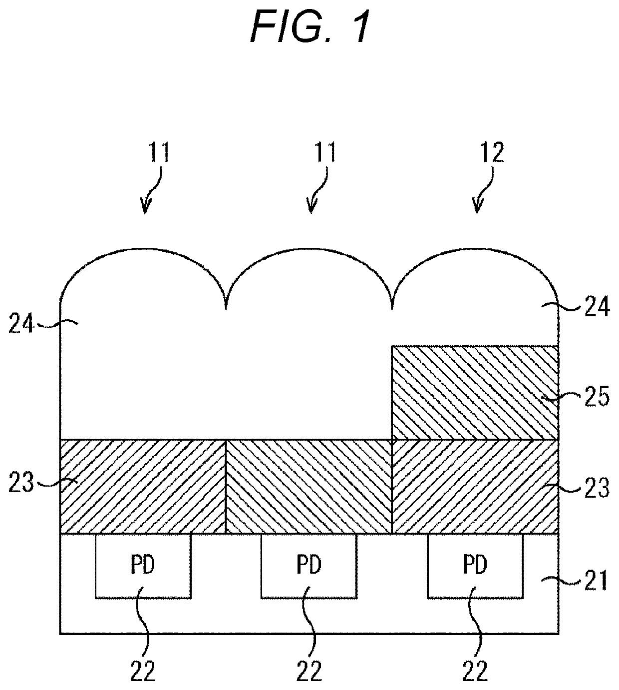
[0111]In a solid-state imaging apparatus 31 according to a first embodiment of the present technology, as a plurality of pixels 32 arranged in a pixel region 33, a visible light pixel and an infrared light pixel are disposed.
[0112]FIG. 4 is a cross-sectional view illustrating a configuration example of a pixel in the solid-state imaging apparatus 31 according to the first embodiment of the present technology. FIG. 4 illustrates a cross-sectional view of a visible light pixel 51 and an infrared light pixel 52 in the solid-state imaging apparatus 31. The visible light pixel 51 is constituted as, for example, three types of pixels of a red (R) pixel, a green (G) pixel, and a blue (B) pixel.
[0113]In the visible light pixel 51, a photoelectric conversion unit 62 constituted by a photodiode (PD) that receives incident light and performs photoelectric conversion is formed on a semiconductor substrate 61. On the semiconductor substrate 61, an insulating layer (not illustr...
second embodiment
4. Second Embodiment
[0203]In a solid-state imaging apparatus 31 according to a second embodiment of the present technology, only visible light pixels are disposed as a plurality of pixels 32 arranged in a pixel region 33.
[0204]FIG. 35 is a cross-sectional view illustrating a configuration example of a pixel in the solid-state imaging apparatus 31 according to the second embodiment of the present technology. FIG. 35 illustrates a cross-sectional view of a visible light pixel 51 in the solid-state imaging apparatus 31. The visible light pixel 51 is constituted as, for example, three types of pixels of a red (R) pixel, a green (G) pixel, and a blue (B) pixel.
[0205]As in the first embodiment, in the visible light pixel 51, a photoelectric conversion unit 62 constituted by a photodiode (PD) that receives incident light and performs photoelectric conversion is formed on a semiconductor substrate 61. On the semiconductor substrate 61, an insulating layer (not illustrated) including SiO or ...
modification example
[0252]As in the first embodiment, also in the present embodiment, the color filter 66 as the second optical filter layer is formed directly on the first optical filter layer.
[0253]The present invention is not limited thereto. As illustrated in FIG. 49, an organic film 111 may be formed between the first optical filter layer (infrared cut filter 63) and the second optical filter layer (color filter 66). Similarly, as illustrated in FIG. 50, an inorganic film 121 may be formed between the first optical filter layer (infrared cut filter 63) and the second optical filter layer (color filter 66).
[0254]Moreover, as illustrated in FIG. 51, an organic film 151 may be formed between the second optical filter layer (color filter 66) and the microlens 67. Similarly, as illustrated in FIG. 52, an inorganic film 161 may be formed between the second optical filter layer (color filter 66) and the microlens 67.
[0255]Note that it is also possible to combine the structure of FIG. 51 or 52 with each o...
PUM
| Property | Measurement | Unit |
|---|---|---|
| wavelength region | aaaaa | aaaaa |
| transmittance | aaaaa | aaaaa |
| height | aaaaa | aaaaa |
Abstract
Description
Claims
Application Information
 - R&D
- Intellectual Property
- Life Sciences
- Materials
- Tech Scout
- Unparalleled Data Quality
- Higher Quality Content
- 60% Fewer Hallucinations
Browse by: Latest US Patents, China's latest patents, Technical Efficacy Thesaurus, Application Domain, Technology Topic, Popular Technical Reports.
© 2025 PatSnap. All rights reserved.Legal|Privacy policy|Modern Slavery Act Transparency Statement|Sitemap|About US| Contact US: help@patsnap.com


