
Scanning signal line drive circuit, display device provided with same, and drive method for scanning signal line

a technology of scanning signal line and drive circuit, which is applied in the direction of static storage, digital storage, instruments, etc., can solve the problems of reducing the speed of pixel capacitor charging, difficult to achieve narrow picture frame areas, and medium- or large-sized display panels that cannot display satisfactory images. , to achieve the effect of reducing or eliminating the difference in scanning signal line drive capability

Active Publication Date: 2020-11-03
SHARP KK
View PDF6 Cites 1 Cited by
  • Summary
  • Abstract
  • Description
  • Claims
  • Application Information

AI Technical Summary

Benefits of technology

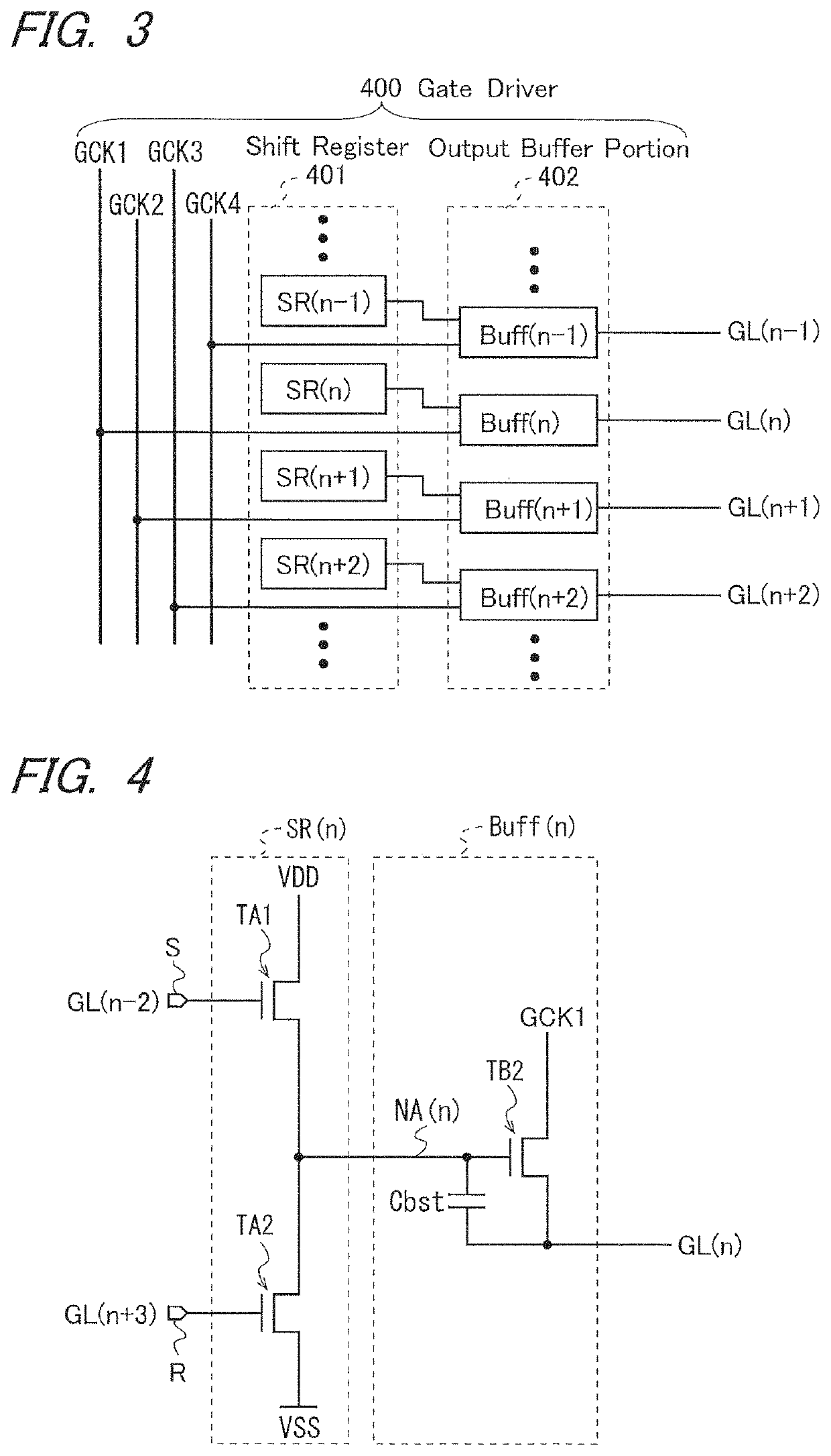
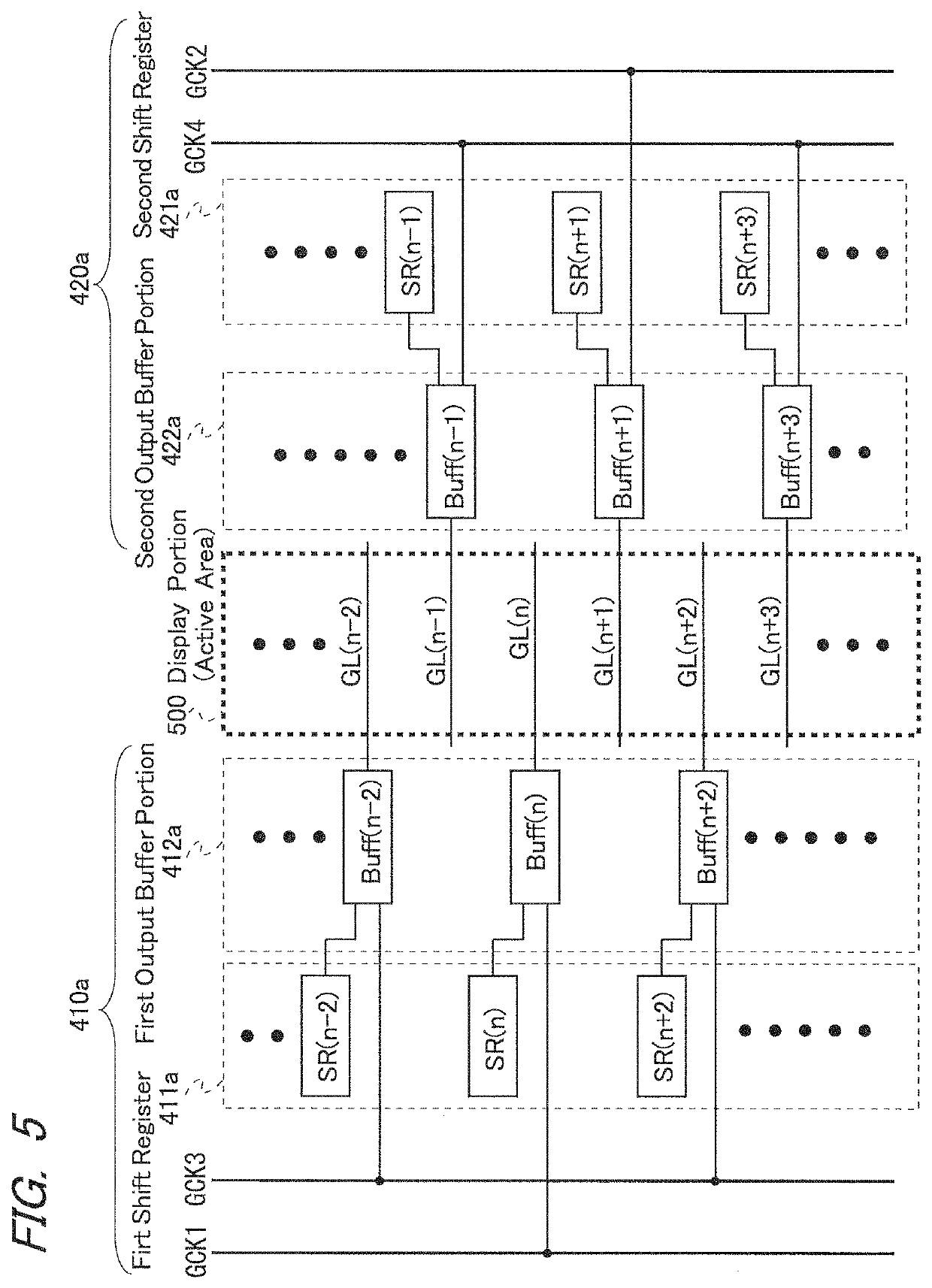
[0028]In this configuration, the scanning signal lines of the display portion are connected at the first ends to buffer circuits in one-to-one correspondence and also at the second ends to other buffer circuits in one-to-one correspondence. Two or more buffer circuits respectively charge or discharge two or more scanning signal lines from their first ends in accordance with an output signal from one first bistable circuit. Two or more other buffer circuits respectively charge or discharge two or more scanning signal lines from their second ends in accordance with an output signal from one second bistable circuit. Thus, it is rendered possible to reduce the area of a shift register, resulting in a display panel with a narrow picture-frame area. Moreover, by charging or discharging the scanning signal lines from both ends, it is rendered possible to drive even a large display portion at high speed. Furthermore, even when there is a difference in charge / discharge capability between buffer circuits corresponding to a single first or second bistable circuit, the first and second bistable circuits output active signals out of phase with each other, with the result that the scanning signal lines are driven uniformly. Thus, it is rendered possible to provide satisfactory display free of artifacts such as stripe patterns.
[0032]the transmission gate is configured to transmit a voltage within a range between a predetermined value corresponding to a power supply voltage for turning on the buffer transistor among power supply voltages for the first and second scanning signal line driver portions and a voltage value for turning off the buffer transistor, and to prevent a voltage that turns on the buffer transistor but is out of the range from being transmitted.
[0040]the transmission gate is configured to transmit a voltage within a range between a predetermined value corresponding to a power supply voltage for turning on the second buffer transistor among power supply voltages for the first and second scanning signal line driver portions and a voltage value for turning off the second buffer transistor, and to prevent a voltage that turns on the second buffer transistor but is out of the range from being transmitted.
[0041](4) Moreover, scanning signal line drive circuits according to several embodiments of the present invention are each a scanning signal line drive circuit including the configuration of above (3), wherein, either or both of different size setting for the first and second transistors and different capacitance value setting for the first and second transistors are performed so as to reduce or eliminate a difference in scanning signal line drive capability between the first-type buffer circuit and the second-type buffer circuit.

Problems solved by technology

However, in the case of the interlaced-arrangement-type gate driver, each gate bus line is provided with a scanning signal from one end, and therefore, the scanning signal suffers from waveform rounding at the other end, resulting in a reduced speed for pixel capacitor charging.
Accordingly, medium- or large-sized display panels have difficulty in displaying satisfactory images using interlaced-arrangement-type gate drivers.
Therefore, relatively large display panels employ the double-ended input scheme as shown in (A) of FIG. 30, which makes it difficult to achieve narrow picture-frame areas.
However, in the liquid crystal display device disclosed in the above publication, the discharge transistor for assisting the discharging of the gate bus line starts transitioning from OFF to ON state after the discharging of the gate bus line is started, and therefore, the discharge transistor cannot perform the discharging at sufficiently high speed.
Moreover, in this liquid crystal display device, the charging of each gate bus line is performed solely by the stage that is coupled to one end of that gate bus line, and therefore, the liquid crystal display device has only low charge capability.
Accordingly, the configuration disclosed in the publication is not suitable for display devices with large display panels.

Method used


Image

  • Scanning signal line drive circuit, display device provided with same, and drive method for scanning signal line
  • Scanning signal line drive circuit, display device provided with same, and drive method for scanning signal line
  • Scanning signal line drive circuit, display device provided with same, and drive method for scanning signal line

Examples


first embodiment

1. First Embodiment

1.1 Overall Configuration and Operation Outline

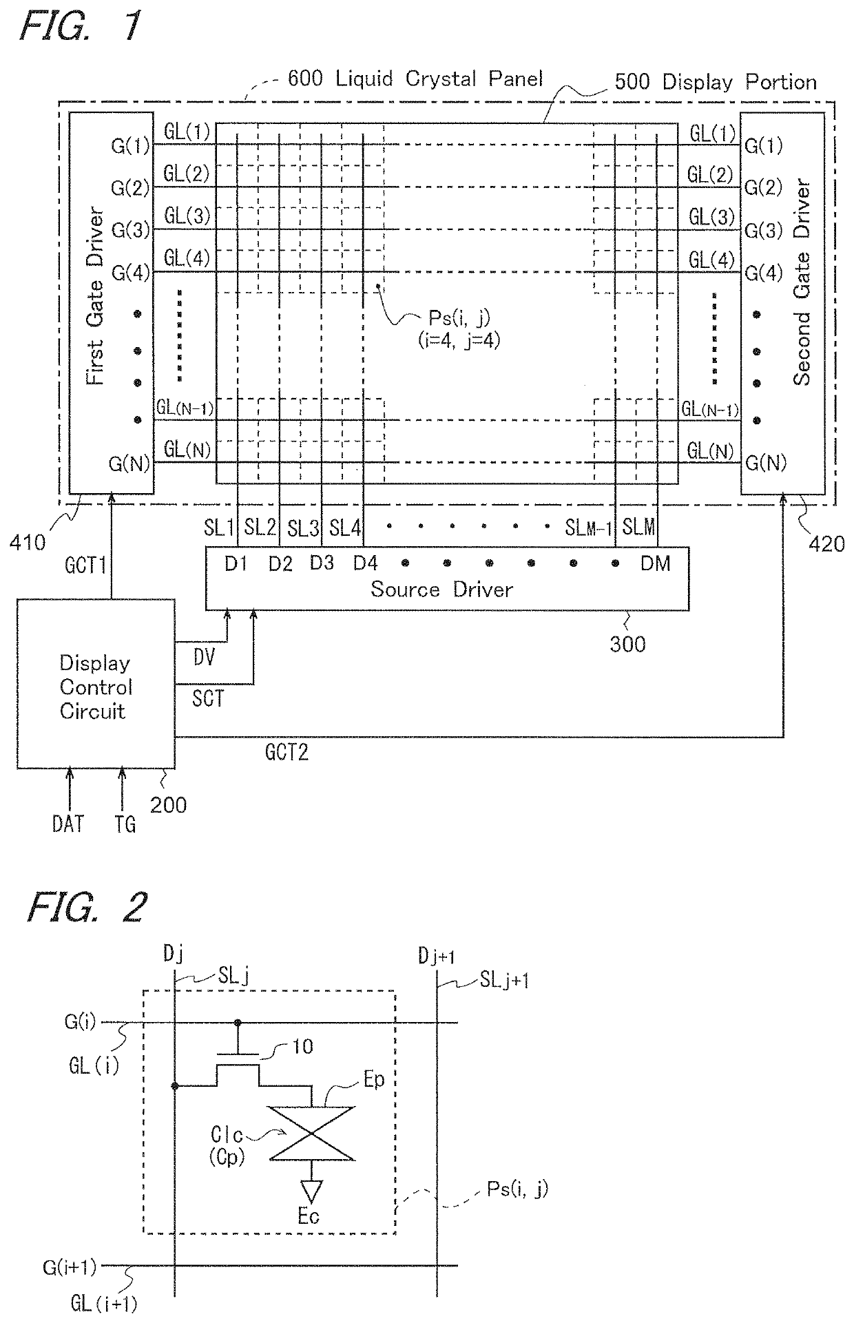
[0106]FIG. 1 is a block diagram illustrating the overall configuration of an active-matrix liquid crystal display device according to the present embodiment. This liquid crystal display device includes a display control circuit 200, a source driver 300 serving as a data signal line drive circuit, and a liquid crystal panel 600, including a display portion 500 and a gate driver serving as a scanning signal line drive circuit. In the present embodiment, pixel circuits included in the display portion 500 and the gate driver are integrally formed on one of two substrates included in the liquid crystal panel 600 (the substrate being referred to as the “active-matrix substrate”), and the gate driver includes first and second gate drivers 410 and 420, which are disposed so as to be opposed to each other with respect to the display portion 500, as shown in FIG. 1.

[0107]The display portion 500 is provided with a plurality (M) ...

second embodiment

2. Second Embodiment

[0165]Next, a display device according to a second embodiment will be described. The display device according to the present embodiment is also an active-matrix liquid crystal display device, and has the same configuration as in the first embodiment, except for the buffer circuits in the gate driver serving as a scanning signal line drive circuit (see FIGS. 1, 2, 6, and 11). In the following, the present embodiment will be described, mainly focusing on the configuration of the buffer circuit in the gate driver, and the other elements, either the same or corresponding elements, are denoted by the same reference characters and will not be elaborated upon.

2.1 Configuration of the Gate Driver

[0166]FIG. 13 is a circuit diagram illustrating the basic configuration of the n'th unit circuit of the gate driver in the present embodiment. The other unit circuits also have the same configuration thereas, except for input and output signals. The basic configuration of the uni...

third embodiment

3. Third Embodiment

[0187]Next, a display device according to a third embodiment will be described. The display device according to the present embodiment is also an active-matrix liquid crystal display device, and has the same configuration as in the first embodiment, except for the buffer circuits in the gate driver serving as a scanning signal line drive circuit (see FIGS. 1, 2, and 6 to 11). In the following, the present embodiment will be described, mainly focusing on the configuration of the buffer circuit in the gate driver, and the other elements, either the same or corresponding elements, are denoted by the same reference characters and will not be elaborated upon.

3.1 Configuration of the Gate Driver

[0188]FIG. 17 is a circuit diagram for describing the basic configuration of the gate driver in the present embodiment and illustrates the configuration of the n'th and (n+1)'th unit circuits for driving the n'th gate bus line GL(n). The n'th unit circuit is included in the first...


PUM


Abstract

An active-matrix display device has a gate driver for driving a plurality of gate bus lines of a display portion in accordance with a multi-phase gate clock signal. The gate driver includes first and second gate drivers disposed to opposite sides of the display portion. Each of the first and second gate drivers includes a plurality of buffer circuits connected to the gate bus lines and a plurality of bistable circuits cascaded together so as to constitute a shift register. Each bistable circuit controls two buffer circuits. The bistable circuits are disposed in an interlaced arrangement between the first and second gate drivers. Each of the two buffer circuits controlled by each bistable circuit includes a boost capacitor, and one of the two buffer circuits includes a transistor for isolating a boost effect.

Description

CROSS REFERENCE TO RELATED APPLICATIONS[0001]This application claims priority to U.S. Provisional Patent Application No. 62 / 750,853, entitled “SCANNING SIGNAL LINE DRIVE CIRCUIT, DISPLAY DEVICE PROVIDED WITH SAME, AND DRIVE METHOD FOR SCANNING SIGNAL LINE”, filed on Oct. 26, 2018, the content of which is incorporated herein by reference.BACKGROUND OF THE INVENTION1. Field of the Invention[0002]The present invention relates to display devices, more specifically to a scanning signal line drive circuit and a drive method, both of which are intended to drive scanning signal lines provided in a display portion of a display device.2. Description of the Related Art[0003]A conventionally known matrix display device is provided with a display portion including a plurality of data signal lines (also referred to as “source bus lines”), a plurality of scanning signal lines (also referred to as “gate bus lines”) crossing the data signal lines, and a plurality of pixel forming portions disposed i...

Claims


Application Information

Patent Timeline
Patent Type & Authority Patents(United States)
IPC IPC(8): G09G3/36
CPCG09G3/3688G09G3/3677G09G2310/0291G09G2310/0286G11C19/28
Inventor TANAKA, KOHHEIWATANABE, TAKUYAIWASE, YASUAKI
Owner SHARP KK
Learn More