Amplification circuit, and receiving circuit, semiconductor apparatus and semiconductor system using the amplification circuit

a technology of amplification circuit and receiving circuit, which is applied in the direction of tone control, gain control, transmission, etc., can solve the problems of ac gain decline and common mode drift of amplification circui

Active Publication Date: 2020-09-15
SK HYNIX INC
View PDF2 Cites 2 Cited by
  • Summary
  • Abstract
  • Description
  • Claims
  • Application Information

AI Technical Summary

Problems solved by technology

Therefore, the common mode of the amplification circuit may drift, or the AC gain may decrease.

Method used


Image

  • Amplification circuit, and receiving circuit, semiconductor apparatus and semiconductor system using the amplification circuit
  • Amplification circuit, and receiving circuit, semiconductor apparatus and semiconductor system using the amplification circuit
  • Amplification circuit, and receiving circuit, semiconductor apparatus and semiconductor system using the amplification circuit

Examples


Embodiment Construction

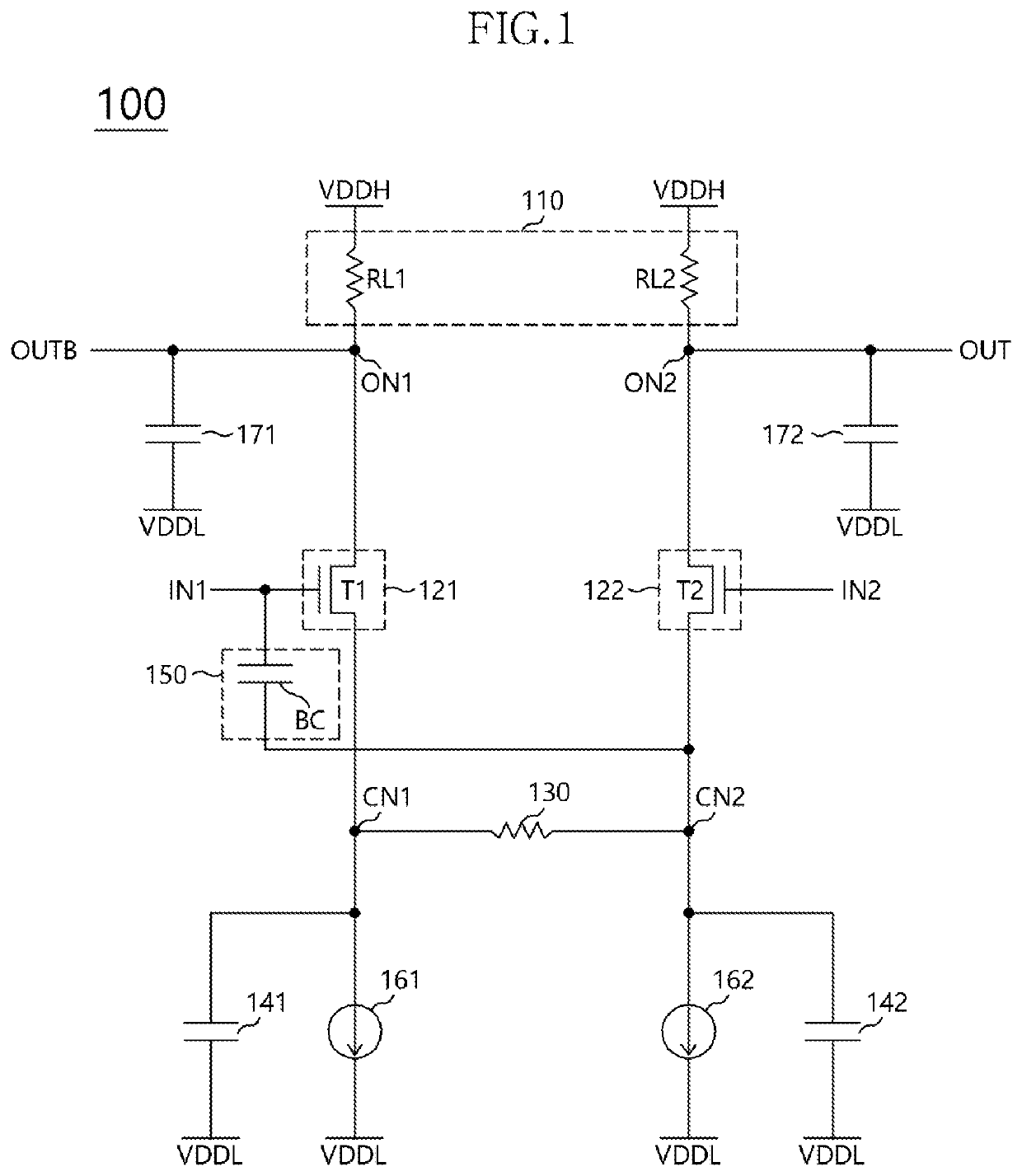
[0013]FIG. 1 illustrates the configuration of an amplification circuit 100 in accordance with an embodiment. The amplification circuit 100 may receive first and second input signals IN1 and IN2 and generate an output signal OUT. The amplification circuit 100 may generate the output signal OUT by differentially amplifying the first and second input signals IN1 and IN2. The amplification circuit 100 may generate a complementary signal OUTB of the output signal with the output signal OUT. In an embodiment, the first and second input signal IN1 and IN2 may be a differential signal pair. For example, the second input signals IN2 may be a complementary signal which is exactly out of phase with the first input signal IN1. In an embodiment, the first input signal IN1 may be a single-ended signal, and the second input signal IN2 may be a reference voltage. The reference voltage may have a voltage level corresponding to the middle of the range in which the first input signal IN1 swings. The a...


PUM


Abstract

An amplification circuit configured to generate an output signal by differentially amplifying first and second input signals. The first and second input signals are a differential signal pair. Alternatively, the first input signal is a single-ended signal, and the second input signal is a reference signal. The amplification circuit is configured to perform a differential amplification operation by increasing a gain for generating an output signal based on the first input signal.

Description

CROSS-REFERENCES TO RELATED APPLICATION[0001]The present application claims priority under 35 U.S.C. § 119(a) to Korean application number 10-2018-0081451, filed on Jul. 13, 2018, in the Korean Intellectual Property Office, which is incorporated herein by reference in its entirety.BACKGROUND1. Technical Field[0002]Various embodiments generally relate to an integrated circuit technology, and more particularly, to a semiconductor apparatus and a semiconductor system.2. Related Art[0003]An electronic device may include many electronic components. Among the electronic components, a computer system may include a large number of semiconductor apparatuses configured as semiconductors. The semiconductor apparatuses constituting the computer system may communicate with one another while transmitting and receiving clocks and data. Each of the semiconductor apparatuses may include a receiving circuit to receive a signal transmitted from an external device or receive a signal transmitted betwee...

Claims


Application Information

Patent Timeline
Patent Type & Authority Patents(United States)
IPC IPC(8): H03F3/45H03F3/193H03G3/30H04B1/16H04B1/04
CPCH03F3/193H03G3/30H03F3/45197H04B1/04H03F2203/45631H03G2201/103H04B1/16H03F2200/378H03F2203/45701H03F2200/372H03G3/007H03G5/28H04B1/123H03G3/008H03G3/3036
Inventor LEE, HYUN BAE
Owner SK HYNIX INC
Why Eureka
Try Eureka