Image sensing device and image sensing method

a technology of image sensing and image, applied in the field of image sensing technique, can solve the problems of increasing the cost, and increasing the cost of image capturing based on such standards, so as to achieve the effect of reducing the cost of hardware configuration

Active Publication Date: 2020-06-23
EAGLE VISION TECH LTD
View PDF20 Cites 0 Cited by
  • Summary
  • Abstract
  • Description
  • Claims
  • Application Information

AI Technical Summary

Benefits of technology

[0005]Exemplary embodiments of the invention provide an image sensing device and an image sensing method. According to the image sensing device and the image sensing method, a plurality of signal converters and a plurality of video encoders compliant with a standard-definition television format are adopted to simultaneously perform signal conversion and signal encoding on high-quality image signals partitioned into a plurality of image areas. Accordingly, the hardware configuration cost is reduced.
[0008]Based on the above, in the image sensing device and the image sensing method according to the embodiments of the invention, the single image sensing array is partitioned into the pixel capturing areas, and multiple signal converters and multiple video encoders compliant with the standard-definition television format (e.g., the NTSC, PAL, and / or SECAM standards) are adopted to convert the image signals obtained in the respective pixel capturing areas into multiple video signals in a specific video format (e.g., the CVBS format). The video decoder configured to receive the video signals generated by the image sensing device may integrate the video signals to obtain a single high-definition digital video signal. Since the technology of the analog-to-digital converter and the video encoder compliant with the standard-definition television format is very matured, and the relevant hardware cost is low, the components (e.g., the analog-to-digital converters and video encoders) are integrated in the same integrated circuit in the embodiment, and the video decoder integrating multiple video signals into a single video signal is also quite accessible, the image sensing device according to the embodiments of the invention has a significantly low hardware configuration cost and may be developed and put into practice within a reduced period of time. Moreover, the size of the single image sensing array according to the embodiments may be laterally expanded to increase the number of pixels, and additional signal converters and image processing apparatuses may be added to process the image pixels increased through lateral expansion. Accordingly, the quality of the image sensed is increased. Besides, the control signals of the respective signal converters and the image processing apparatuses are the same, so it does not require other control signals. Furthermore, the single image sensing array is in fact not separated and is integrally disposed in the same integrated circuit, whereas different components are adopted to simultaneously process different pixel capturing areas on the single image sensing array when signal conversion and image processing are carried out. Therefore, the video signals obtained through processing are able to be integrated smoothly without generating twisted or deformed images. In other words, in the embodiments of the invention, the pixels sensed by the image sensing array are read through a plurality of partitioned blocks (e.g., a plurality of pixel capturing areas), but the overall pixels of a sensed image is coherent and complete. Besides, the process of reading pixels by the image sensing array according to the embodiments of the invention does not affect the physical uniformity of the overall pixels of the sensed image. Moreover, the pixel reading speed is facilitated and the configuration cost is reduced.

Problems solved by technology

However, the resolutions of images captured based on such standards is gradually unable to satisfy the high-resolution demands for image capturing.
Thus, the cost becomes higher.
There are not many manufacturers integrating analog-to-digital signal conversion and image encoding in a single chip.

Method used


Image

  • Image sensing device and image sensing method
  • Image sensing device and image sensing method
  • Image sensing device and image sensing method

Examples


first embodiment

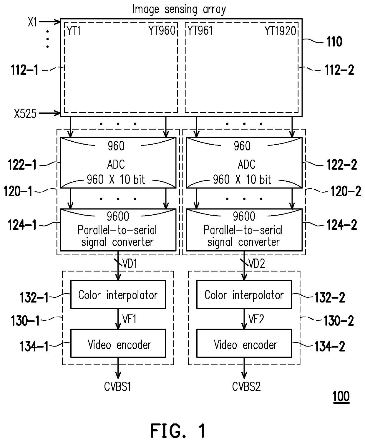
[0020]FIG. 1 is a block diagram illustrating an image sensing device 100 according to the invention. The image sensing device 100 mainly includes an image sensing array 110, a plurality of first signal converters 120-1 and 120-2, and a plurality of first image processing apparatuses 130-1 and 130-2. The image sensing device 100 of the embodiment is applicable in an information system or an electronic apparatus relating to image capturing, such as a surveillance apparatus, a security system and / or the like.

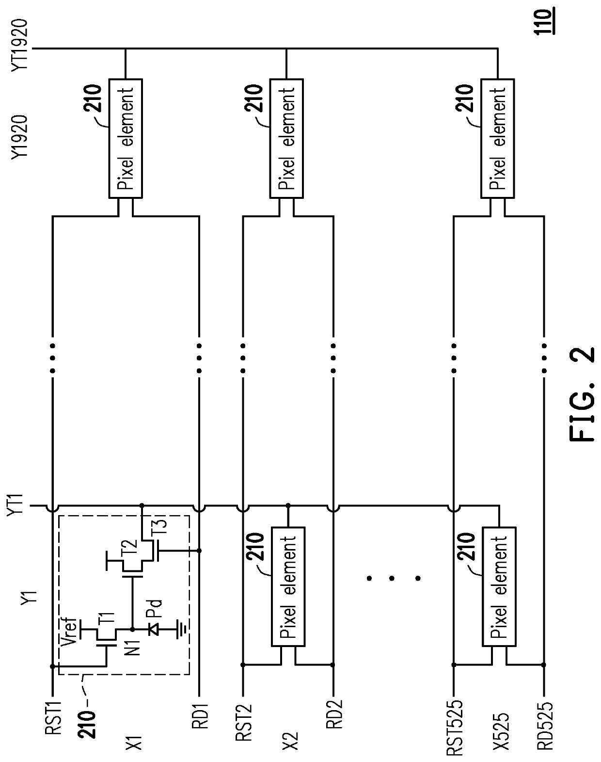
[0021]FIG. 2 is a schematic view illustrating the image sensing array 110 of FIG. 1. Referring to FIG. 2, the image sensing array 110 includes a plurality of pixel elements 210 arranged into columns and rows. The pixel element 210 of the embodiment may include a photodiode Pd and transistors T1 to T3. Assuming that an interlaced scanning system complies with the American National Television System Committee (NTSC) standard, an image may be displayed by being partitioned into odd an...

second embodiment

[0032]FIG. 4 is a block diagram illustrating an image sensing device 400 according to the invention. Compared with FIG. 1, the image sensing device 400 includes an image sensing array in a larger size (i.e., 1050×1920 pixels) and further includes another set of image sensing apparatus in addition to the image sensing apparatus 100 having the first signal converters 120-1 and 120-2 and the first image processing apparatuses 130-1 and 130-2. In other words, the image sensing device 400 further includes a plurality of second signal converters 420-1 and 420-2 and a plurality of second image processing apparatuses 430-1 and 430-2.

[0033]The second signal converters 420-1 and 420-2 and the second image processing apparatuses 430-1 and 430-2 share similar functions and circuit structures with the first signal converter 120-1 and 120-2 and the first image processing apparatuses 130-1 and 130-2 shown in FIG. 1. In addition to the image capturing areas 112-1 and 112-2, the image sensing array ...

third embodiment

[0037]FIG. 5 is a block diagram illustrating an image sensing device 500 according to the invention. What FIG. 5 differs from FIG. 4 is that an image sensing array 510 of the image sensing device 500 of FIG. 5 is in a size of 1050×2880 pixels. Compared with the image sensing array 410 (1050×1920 pixels), the image sensing array 510 is expanded laterally by a certain number of pixels. Therefore, in addition to the pixel capturing areas 112-1, 112-2, 412-1 and 412-2, the image sensing array 510 further includes additional pixel capturing areas 512-1 and 512-2 partitioned in the image sensing array 510. Accordingly, the image sensing device 500 according to an embodiment of the invention may additionally include a plurality of signal converters (e.g., signal converters 520-1 and 520-2) and a plurality of image processing apparatuses (e.g., image processing apparatuses 530-1 and 530-2) to simultaneously process pixels newly added through lateral expansion, such as simultaneously reading...


PUM


Abstract

An image sensing device and an image sensing method are provided. The image sensing device includes an image sensing array, multiple first signal converters, and multiple first image processing apparatuses. The image sensing array is partitioned into at least two or more first pixel capturing areas, and each of the first pixel capturing areas is compliant with a resolution of an SDTV format. Each of the first signal converters receives an analog image signal from a corresponding first pixel capturing area, converts the analog image signal from an analog format to a digital format to generate a first digital image signal, and converts the first digital image signal from an parallel format to a serial format. Each of the image processing apparatuses is configured to convert the first digital image signal in the serial format of a corresponding first signal converter to a video signal in a specific video format.

Description

CROSS-REFERENCE TO RELATED APPLICATION[0001]This application claims the priority benefit of Taiwan application serial no. 106122032, filed on Jun. 30, 2017. The entirety of the above-mentioned patent application is hereby incorporated by reference herein and made a part of this specification.BACKGROUND OF THE INVENTION1. Field of the Invention[0002]The invention relates to an image sensing technique, and particularly relates to an image sensing device and an image sensing method for high-quality image sensing and video encoding by a plurality of analog-digital signal converters and a plurality of video encoders compliant with a standard-definition television format.2. Description of Related Art[0003]Owing to the continuously improved image sensing techniques, the image quality captured by a conventional image sensing system is also becoming better. A conventional analog image sensing system generally complies with a standard-definition television format, e.g., the American National ...

Claims


Application Information

Patent Timeline
Patent Type & Authority Patents(United States)
IPC IPC(8): H04N5/378H04N9/04H04N5/374H04N5/225H04N5/232H03M1/10H03M1/66H04N19/40H04N7/18H04N5/369H01L27/146
CPCH04N5/379H01L27/14603H04N19/40H04N7/183H04N7/18H04N9/045H04N5/23232H04N5/2258H04N5/378H04N5/23229H04N5/268H04N21/4402H04N21/440218H04N23/45H04N23/951H04N25/79H04N23/10H04N25/75H04N23/80
Inventor LEE, SYWE-NENG
Owner EAGLE VISION TECH LTD
Why Eureka
Try Eureka