
Image processing sensor

a technology of image processing and sensor, applied in the field of image processing sensor, can solve the problems of low heat resistance of the above-mentioned unit, impaired normal operation of the display unit, etc., and achieve the effect of accurately and easily achieving setting operation and confirming images of target objects

Active Publication Date: 2019-09-24
KEYENCE
View PDF3 Cites 2 Cited by
  • Summary
  • Abstract
  • Description
  • Claims
  • Application Information

AI Technical Summary

Benefits of technology

The invention aims to provide an image processing sensor that enables users to accurately and easily set up the sensor and confirm images of target objects.

Problems solved by technology

Generally, however, the display unit described above that displays images does not have high heat resistance.
Therefore, when heat generated by the plurality of light-emitting elements and the camera module is transferred to the display unit, a normal operation of the display unit may be impaired.

Method used


Image

  • Image processing sensor
  • Image processing sensor
  • Image processing sensor

Examples


Embodiment Construction

[1] Basic Configuration and Basic Operation of Image Processing Sensor

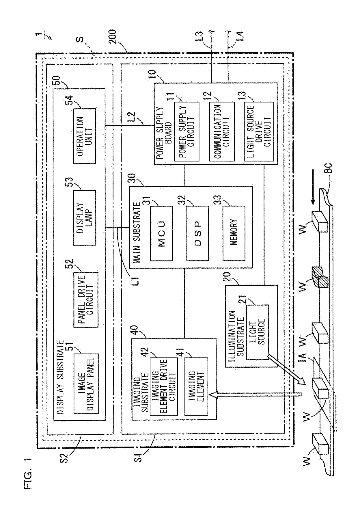
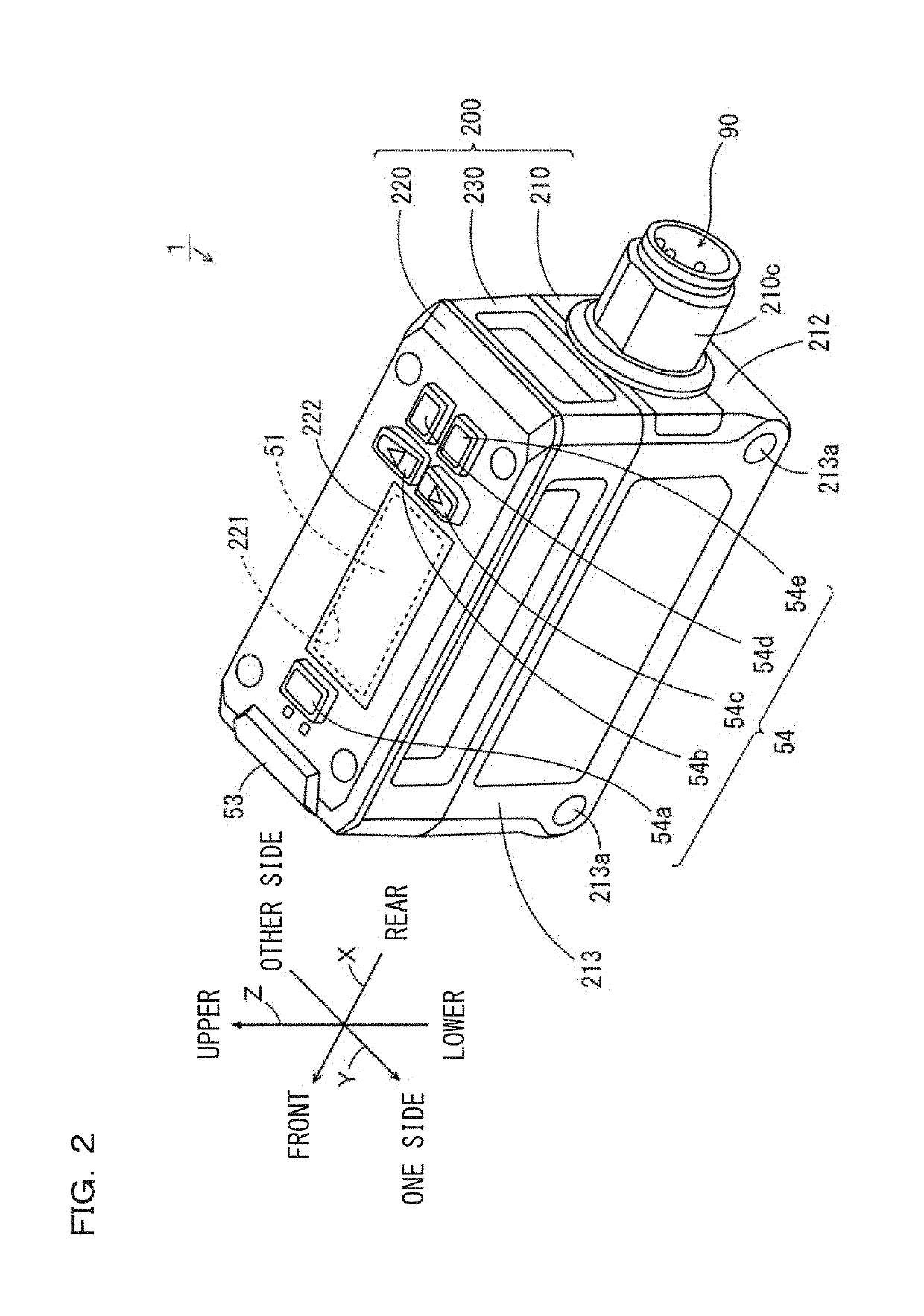
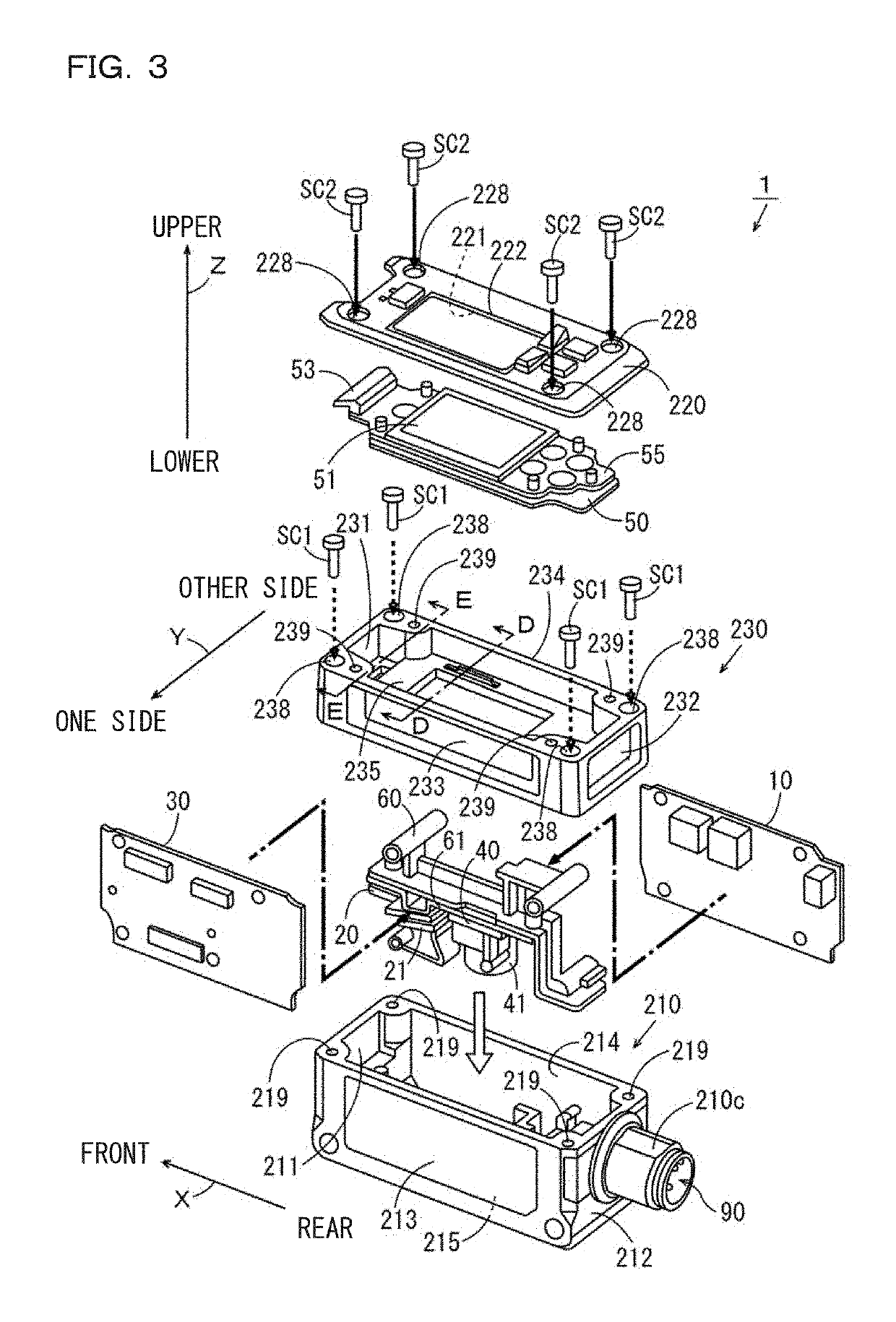
[0070]FIG. 1 is a block diagram illustrating a basic configuration of an image processing sensor according to an embodiment of the invention. As illustrated in FIG. 1, an image processing sensor 1 has a configuration in which a power supply board 10, an illumination substrate 20, a main substrate 30, an imaging substrate 40, and a display substrate 50 are housed in an internal space S of a casing 200.

[0071]The power supply board 10 is electrically connected to the illumination substrate 20, the main substrate 30, and the display substrate 50 via wiring members. The main substrate 30 is electrically connected to the imaging substrate 40 and the display substrate 50 via the wiring members. In this example, a flexible wiring circuit board is used as a wiring member L1 out of a plurality of the wiring members for coupling the main substrate 30 and the display substrate 50. A harness is used as a wiring member L2 for c...


PUM


Abstract

An image processing sensor which enables users to perform a setting operation accurately and easily while confirming an image of a target object is provided.The image processing sensor has a configuration in which a power supply board, an illumination substrate, a main substrate, an imaging substrate, and a display substrate are housed in an internal space of a casing. The casing includes a first casing member, a second casing member, and a coupling casing member. The coupling casing member is interposed between the first casing member and the second casing member.

Description

CROSS-REFERENCE TO RELATED APPLICATIONS[0001]The present application claims foreign priority based on Japanese Patent Application No. 2016-106638, filed May 27, 2016, the contents of which is incorporated herein by reference.BACKGROUND OF THE INVENTION1. Field of the Invention[0002]The present invention relates to an image processing sensor.2. Description of Related Art[0003]In factory production lines, image processing sensors are used for determining presence or absence of positional deviation or defects of target objects that are conveyed by a belt conveyor or the like (For example, see JP-A-2013-109508).[0004]In an image processing device described in JP-A-2013-109508, a plurality of light-emitting elements and a camera module are integrally housed in a single case. Lights are emitted from the plurality of light-emitting elements to a target object, and the target object is imaged by the camera module. Based on an image acquired by imaging, pass / fail determination of the corresp...

Claims


Application Information

Patent Timeline
Patent Type & Authority Patents(United States)
IPC IPC(8): H04N5/225G06T7/73G03B43/00G03B17/55G03B17/02H04N5/232G06T7/00
CPCH04N5/2256G06T7/74G03B43/00H04N5/2252G03B17/02G06T7/001H04N5/2253H04N5/23293G03B17/55G06T2207/20081G06T2207/10004G06T2207/30164H04N23/53H04N23/51H04N23/54H04N23/56
Inventor KIDA, DAISUKE
Owner KEYENCE
Learn More