
Separation apparatus, separation system, and separation method

a separation apparatus and separation system technology, applied in the direction of chemistry apparatus and processes, layered products, other domestic articles, etc., can solve the problems of large time required to separate the wafer and the supporting substrate, the wafer has been made thinner and is therefore susceptible to damage, and the damage is large, so as to achieve the effect of appropriate and efficient separation processing of the processing target substrate and the supporting substra

Active Publication Date: 2018-09-11
INTEL CORP
View PDF17 Cites 0 Cited by
  • Summary
  • Abstract
  • Description
  • Claims
  • Application Information

AI Technical Summary

Benefits of technology

[0008]The present invention has been made in consideration of the above point, and an object thereof is to appropriately and efficiently perform separation processing of a processing target substrate and a supporting substrate.
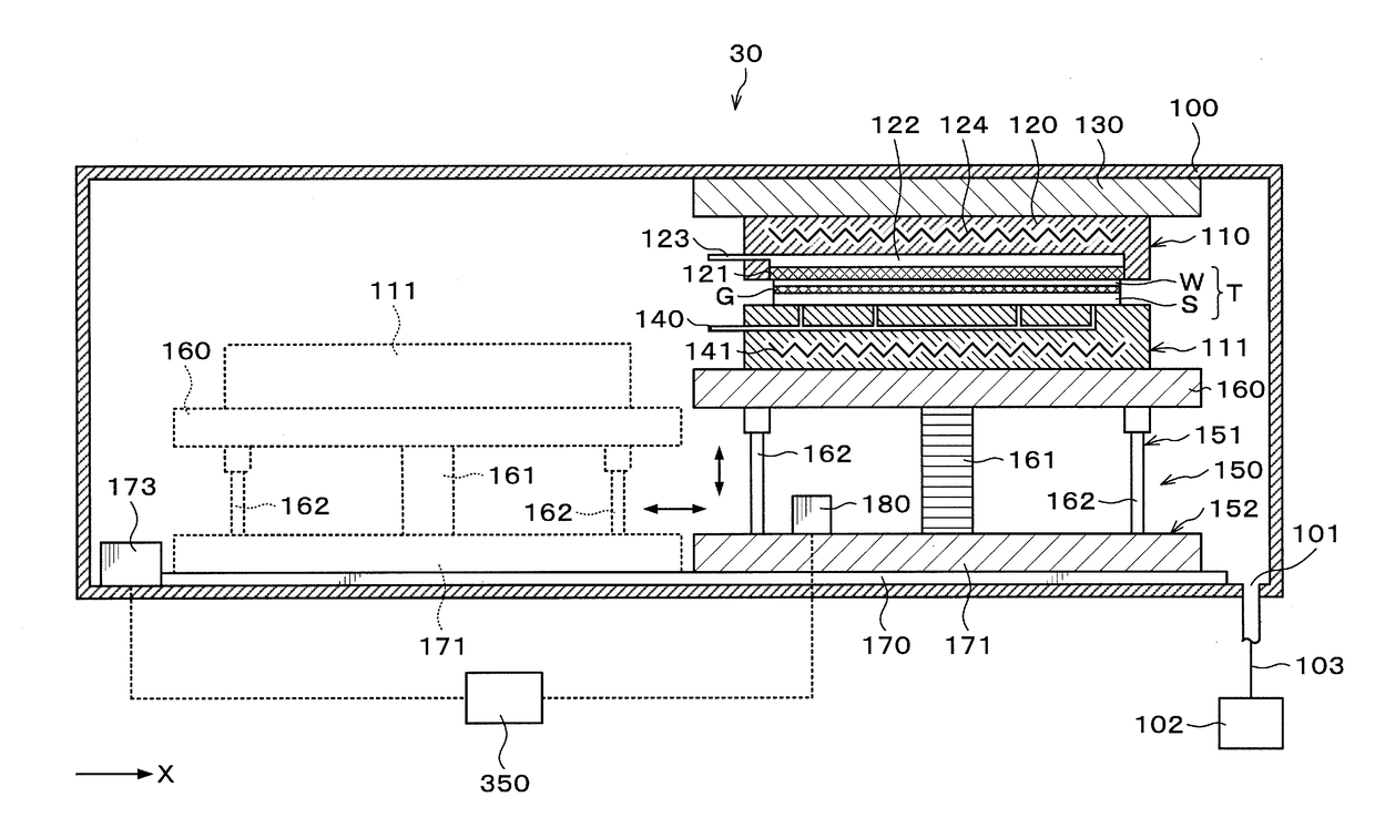
[0010]According to the present invention, the moving mechanism relatively moves the first holding unit or the second holding unit in a horizontal direction to separate the processing target substrate and the supporting substrate. Then, a load acting on the processing target substrate and the supporting substrate is measured by the load measurement unit when the processing target substrate and the supporting substrate are separated, and the moving mechanism is controlled based on the load measured by the load measurement unit. Since the moving mechanism can be feedback-controlled as described above, an appropriate load can be made to act on the processing target substrate and the supporting substrate. As a result, the damage to the processing target substrate and the supporting substrate can be suppressed. Further, it is possible to optimize the time required to separate the processing target substrate and the supporting substrate, thereby improving the throughput of the separation processing. As described above, according to the present invention, it is possible to appropriately and efficiently perform the separation processing of the processing target substrate and the supporting substrate.
[0013]According to the present invention, it is possible to appropriately and efficiently perform separation processing of a processing target substrate and a supporting substrate.

Problems solved by technology

However, in the case of using the separation apparatus described in Patent Document 1, the liquid is jetted at a high jetting pressure and may therefore damage the wafer or the supporting substrate.
In particular, the wafer has been made thinner and is thus susceptible to damage.
However, in this case, a lot of time is required to separate the wafer and the supporting substrate.

Method used


Image

  • Separation apparatus, separation system, and separation method
  • Separation apparatus, separation system, and separation method
  • Separation apparatus, separation system, and separation method

Examples


Embodiment Construction

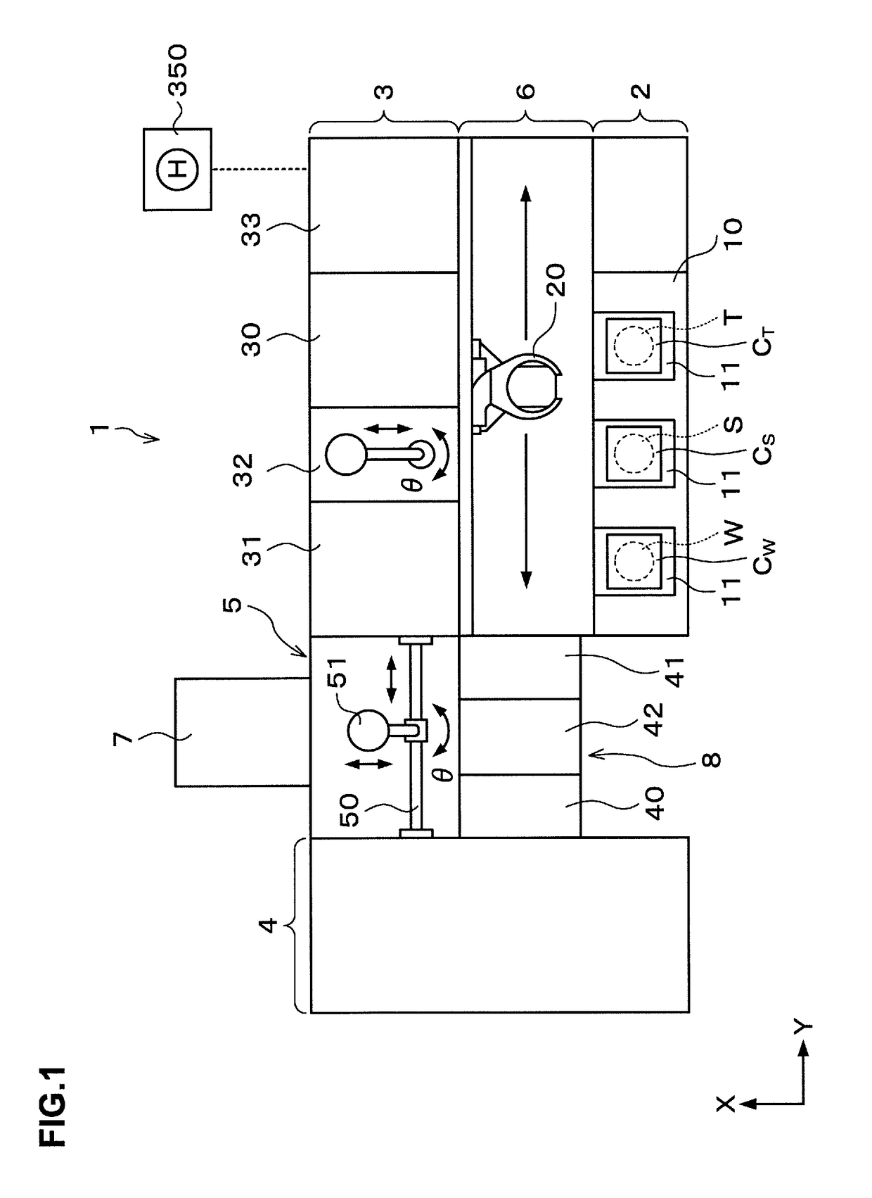
[0039]Hereinafter, embodiments of the present invention will be described. FIG. 1 is a plan view illustrating the outline of a configuration of a separation system 1 according to an embodiment.

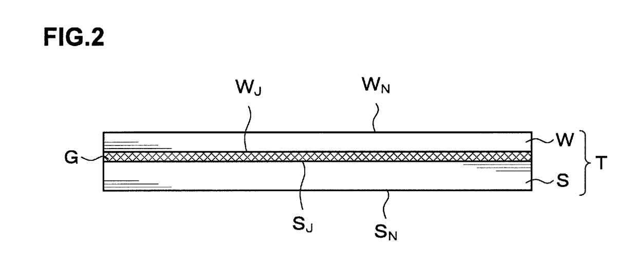
[0040]In the separation system 1, a superposed wafer T as a superposed substrate in which a processing target wafer W as a processing target substrate and a supporting wafer S as a supporting substrate are joined together with an adhesive G as illustrated in FIG. 2 is separated into the processing target wafer W and the supporting wafer S. Hereinafter, in the processing target wafer W, the surface to be joined with the supporting wafer S via the adhesive G is referred to as a “joint surface WJ” and the surface opposite to the joint surface WJ is referred to as “a non-joint surface WN.” Similarly, in the supporting wafer S, the surface to be joined with the processing target wafer W via the adhesive G is referred to as a “joint surface SJ” and the surface opposite to the joint surface SJ is ref...


PUM

PropertyMeasurementUnit
thicknessaaaaaaaaaa
temperatureaaaaaaaaaa
thicknessaaaaaaaaaa

Abstract

A separation apparatus for separating a superposed substrate in which a processing target substrate and a supporting substrate are joined together with an adhesive, into the processing target substrate and the supporting substrate, includes: a first holding unit which holds the processing target substrate; a second holding unit which holds the supporting substrate; a moving mechanism which relatively moves the first holding unit or the second holding unit in a horizontal direction; a load measurement unit which measures a load acting on the processing target substrate and the supporting substrate when the processing target substrate and the supporting substrate are separated; and a control unit which controls the moving mechanism based on the load measured by the load measurement unit.

Description

BACKGROUND OF THE INVENTION[0001]1. Field of the Invention[0002]The present invention relates to a separation apparatus for separating a superposed substrate into a processing target substrate and a supporting substrate, a separation system including the separation apparatus, and a separation method using the separation apparatus.[0003]2. Description of the Related Art[0004]In recent years, for example, in a manufacturing process of a semiconductor device, the diameter of a semiconductor wafer (hereinafter, referred to as a “wafer”) increasingly becomes larger. Further, the wafer is required to be thinner in a specific process such as mounting. When a thin wafer with a large diameter is transferred or subjected to polishing as it is, warpage or break can occur in the wafer. Therefore, in order to reinforce the wafer, for example, bonding the wafer to a wafer being a supporting substrate or a glass substrate is performed. The predetermined processing such as polishing and the like ar...

Claims


Application Information

Patent Timeline
Patent Type & Authority Patents(United States)
IPC IPC(8): B32B38/10H01L21/67B32B43/00
CPCB32B38/10H01L21/67051H01L21/67092H01L21/67288Y10T156/1972B32B2457/14Y10T156/11Y10T156/1189Y10T156/19B32B43/006H01L21/02H01L21/30
Inventor HIRAKAWA, OSAMUHONDA, MASARUFUKUTOMI, AKIRATAMURA, TAKESHIHARADA, JIRONODA, KAZUTAKABRUN, XAVIER FRANCOIS
Owner INTEL CORP
Learn More