
Substrate structure

a substrate and structure technology, applied in the field of substrate structures and display devices, can solve the problems of unsatisfactory optical characteristics (e.g., transmittance) of the oled device, insufficient electron mobility of the tft, and unsatisfactory performance of the tft, so as to achieve satisfactory light transmittance of the substrate structure, minimize the differences of refractive indexes in the substrate structure, and easy to break

Active Publication Date: 2018-07-10
SAMSUNG DISPLAY CO LTD
View PDF9 Cites 2 Cited by
  • Summary
  • Abstract
  • Description
  • Claims
  • Application Information

AI Technical Summary

Benefits of technology

The solution achieves satisfactory light transmittance and improved electron mobility of the transistor, ensuring better performance and optical characteristics.

Problems solved by technology

The insulation layers may cause optical characteristics (e.g., transmittance) of the OLED device to be unsatisfactory.
As a result, electron mobility of the TFT may insufficient, and thus performance of the TFT may be unsatisfactory.

Method used


Image

  • Substrate structure
  • Substrate structure
  • Substrate structure

Examples


Embodiment Construction

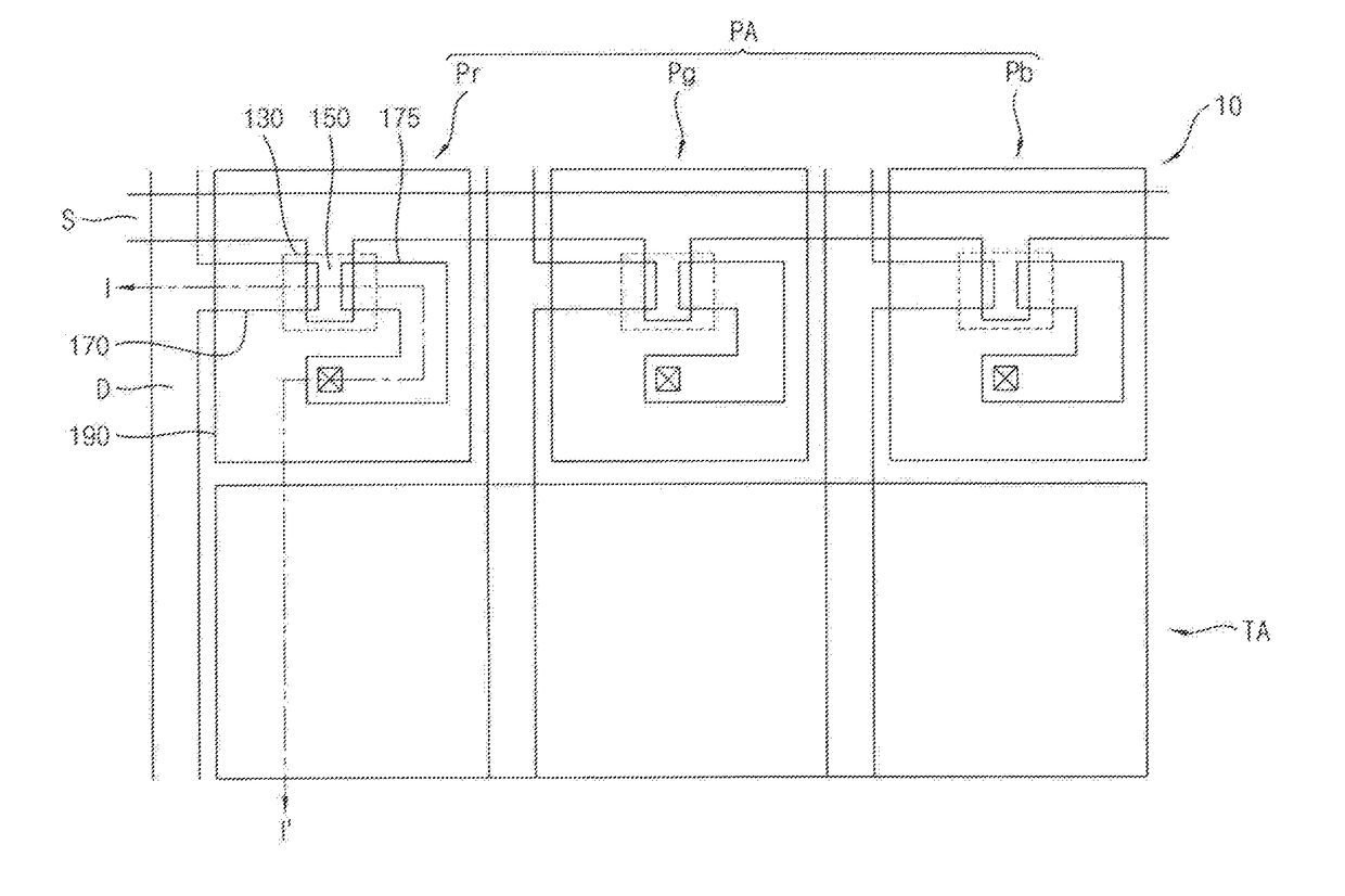
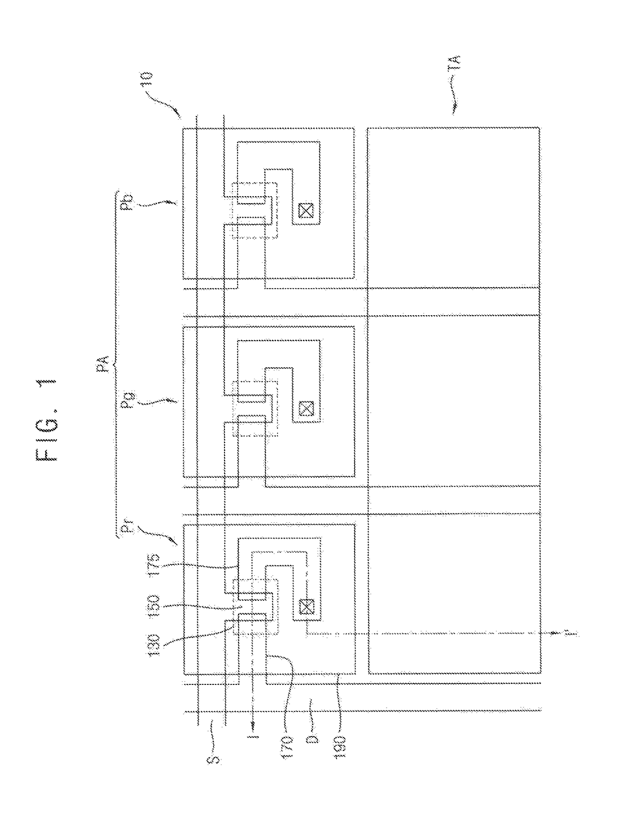
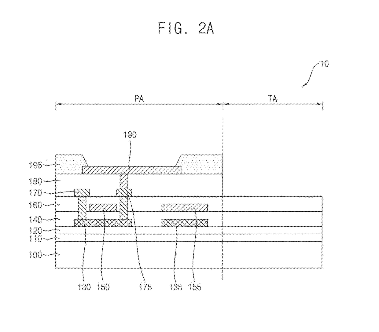
[0056]Display devices, e.g., transparent display devices, and methods of manufacturing display devices in accordance with example embodiments are explained in detail with reference to the accompanying drawings.

[0057]Although the terms “first”, “second”, etc. may be used herein to describe various elements, these elements should not be limited by these terms. These terms may be used to distinguish one element from another element. Thus, a first element discussed in this application may be termed a second element without departing from embodiments. The description of an element as a “first” element may not require or imply the presence of a second element or other elements. The terms “first”, “second”, etc. may also be used herein to differentiate different categories or sets of elements. For conciseness, the terms “first”, “second”, etc. may represent “first-category (or first-set)”, “second-category (or second-set)”, etc., respectively.

[0058]The term “connect” may mean “mechanically...


PUM


Abstract

A substrate structure may be used in a display device. The substrate structure may include a base substrate, a transistor, and a silicon oxynitride layer. The transistor may include a semiconductor member and a gate electrode and may overlap the base substrate. The silicon oxynitride layer may directly contact at least one of the base substrate, the semiconductor member, and the gate electrode and may include (and / or contain) a hydrogen atom set. A hydrogen concentration in the silicon oxynitride layer may be greater than or equal to 1.52 atomic percent.

Description

CROSS-REFERENCE TO RELATED APPLICATION(S)[0001]This application claims priority under 35 USC § 119 to Korean Patent Application No. 10-2015-0143067, filed on Oct. 13, 2015 in the Korean Intellectual Property Office (KIPO); the entire disclosure of the Korean Patent Application is incorporated by reference herein.BACKGROUND[0002]1. Field[0003]Example embodiments relate to substrate structures and display devices.[0004]2. Description of the Related Art[0005]A display device, e.g., an organic light-emitting display (OLED) device may include a stack of insulation layers that contain different materials. The insulation layers may cause optical characteristics (e.g., transmittance) of the OLED device to be unsatisfactory.[0006]An active member of a thin film transistor (TFT) included in the display device may be influenced by insulation layers disposed on and / or under the active member. As a result, electron mobility of the TFT may insufficient, and thus performance of the TFT may be unsa...

Claims


Application Information

Patent Timeline
Patent Type & Authority Patents(United States)
IPC IPC(8): H01L27/14H01L51/52H01L27/32H10K99/00
CPCH01L27/3258H01L51/5253H01L27/3262H01L27/326H01L29/7869H01L27/1218H01L27/1248H01L27/1255H10K59/124H10K59/121H10K59/1213H10K59/873H10K50/844
Inventor CHUNG, YUNG-BINJEON, BO-GEONCHO, EUN-JEONGPARK, HYE-HYANGYANG, SUNG-HOONJEON, WOO-SEOKJEON, JOO-HEECHOI, CHAUN-GI
Owner SAMSUNG DISPLAY CO LTD
Learn More