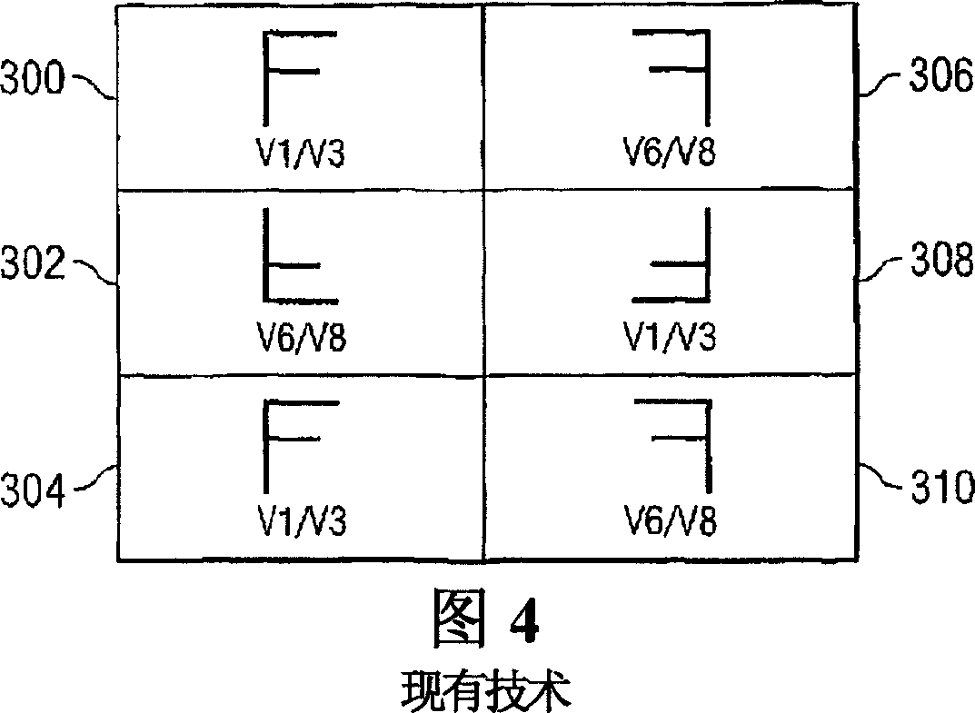
Staggered memory cell array

一种存储器单元、阵列的技术,应用在静态存储器、数字存储器信息、信息存储等方向,能够解决阵列尺寸限制等问题

Inactive Publication Date: 2007-05-09
TEXAS INSTR INC
View PDF0 Cites 2 Cited by
  • Summary
  • Abstract
  • Description
  • Claims
  • Application Information

AI Technical Summary

Problems solved by technology

Therefore, the size of a single memory cell and the corresponding array size is limited by these critical dimensions

Method used


Image

  • Staggered memory cell array
  • Staggered memory cell array
  • Staggered memory cell array

Examples


Embodiment Construction

[0030]Referring to FIG. 17, there is shown a block diagram of a radiotelephone as an example of a portable electronic device that may advantageously use the present invention for memory arrays, decoding circuits, interconnection units, or any other known in the art. in other geometric arrays. The radiotelephone includes antenna 1700 , radio frequency transceiver 1702 , baseband circuitry 1710 , microphone 1706 , speaker 1708 , keypad 1720 and display 1722 . The radiotelephone is preferably powered by a rechargeable battery (not shown) as is well known in the art. Antenna 1700 enables the radiotelephone to interact with the radio frequency environment in a manner known in the art for wireless communication. The radio frequency transceiver 1702 transmits and receives radio frequency signals through the antenna 1702 . The transmitted signal is modulated by the voice / data output signal received from the baseband circuit 1710 . The received signal is demodulated and provided to ...


PUM


Abstract

A method of placing a cell in an array is disclosed. The method includes placing the cell a plurality of times (600, 602, 604) in a first array. The cell is also placed a plurality of times (606, 608, 610) in a second array. The second array is placed adjacent and offset from the first array by an offset distance (O2).

Description

technical field [0001] The present invention relates generally to electronic circuits, and more particularly to geometry efficiency of semiconductor integrated circuits. Background technique [0002] The growing popularity of portable electronic devices poses enormous challenges to manufacturers. The ever-increasing capabilities of electronic devices are constrained by considerations such as cost, size, weight, and battery life. These considerations have led to higher and higher integration levels of semiconductors. Therefore, portable electronic devices often embed memory, control functions, signal processors, and other circuit functions on a single integrated circuit. Further optimization of these portable electronic devices requires even further reductions in geometry size and the space between these geometries. However, reducing the geometric size and space of semiconductor integrated circuits is limited by state-of-the-art manufacturing equipment. Reducing geometry ...

Claims


Application Information

Patent Timeline
Patent Type & Authority Applications(China)
IPC IPC(8): G11C5/06H01L27/11
CPCH01L27/1104H10B10/12G11C5/06G11C7/10
Inventor 凯范·萨德拉狄奥多尔·W·休斯顿
Owner TEXAS INSTR INC
Why Eureka
Try Eureka