Novel compound and organic electronic device using such compound
A compound and organic group technology, applied in the field of organic solar cells, can solve the problems of inability to transport photocarriers, unstable discharge compared to positive polarity, adverse effects of the use environment, etc., and achieve excellent film stability and excellent electron transfer properties Effect
- Summary
- Abstract
- Description
- Claims
- Application Information
AI Technical Summary
Problems solved by technology
Method used
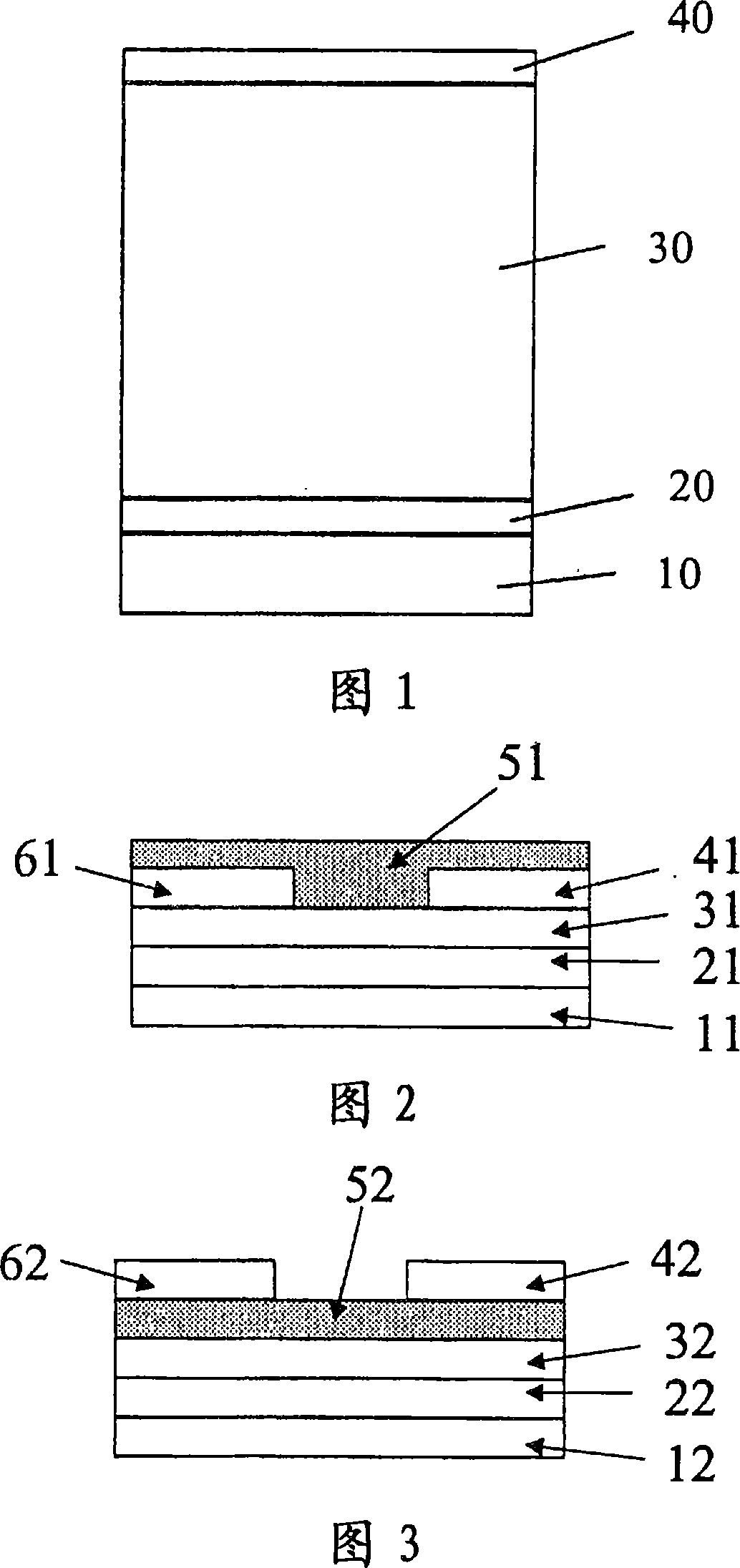
Image

Examples
Embodiment 1
[0347]
[0348] Synthesis of naphthalene monoimide (1-1) in the first step
[0349] The reaction container containing 8.0 g of naphthalene-1,4,5,8-tetracarboxylic dianhydride and 50 ml of dehydrated DMF was charged under reflux under heating. Then, 30 ml of dehydrated DMF dissolved in 3.85 g of 2-ethylhexylamine was added dropwise while stirring. After the dropwise addition was completed, it was further heated to reflux for 6 hours. After cooling, it was concentrated under reduced pressure, the residue was diluted with toluene, and the insoluble components were filtered off. Purify by silica gel chromatography to obtain the target naphthalene monoimide (1-1). Yield: 3.89g.
[0350] The second step synthesizes naphthalene monoimide monohydrazone derivatives (1-2)
[0351] 12.0 g of naphthalene-1,4,5,8-tetracarboxylic dianhydride and 60 ml of dehydrated DMF were placed in the reaction container heated to reflux. Then, 5.78 g of 2-aminooctane was dissolved in 30 ml of deh...
Embodiment 2
[0358]
[0359] Synthesis of naphthalene monoimide (2-1) in the first step
[0360] The reaction container containing 27.0 g of naphthalene-1,4,5,8-tetracarboxylic dianhydride and 250 ml of dehydrated DMF was charged under reflux under heating. Then, 9.0 g of 3-aminopentane was dissolved in 100 ml of dehydrated DMF dropwise over 30 minutes while stirring. After the dropwise addition was completed, it was further heated to reflux for 6 hours. After cooling, it was concentrated under reduced pressure, the residue was diluted with toluene, and the insoluble components were filtered off. Purification was carried out by silica gel column chromatography to obtain the light yellow target monoimide (2-1). Yield: 13.3g.
[0361] The second step synthesizes naphthalene monoimide monohydrazone derivatives (2-2)
[0362] 10.0 g of the naphthalene monoimide (2-1) obtained above and 100 ml of dehydrated DMF were charged and dissolved. Then, 1.65 g of hydrazine monohydrate was added dr...
Embodiment 3
[0367]
[0368] Synthesis of naphthalene monoimide (3-1) in the first step
[0369] The reaction container containing 42.0 g of naphthalene-1,4,5,8-tetracarboxylic dianhydride and 400 ml of dehydrated DMF was charged under reflux under heating. Then, 18.9 g of 2-heptylamine was dissolved in 100 ml of dehydrated DMF dropwise over 50 minutes while stirring. After the dropwise addition was completed, it was further heated to reflux for 6 hours. After cooling, it was concentrated under reduced pressure, the residue was diluted with toluene, and the insoluble components were filtered off. Purify by silica gel column chromatography to obtain the light yellow target monoimide (3-1). Yield: 25.3g.
[0370] The second step synthesizes naphthalene monoimide monohydrazone derivatives (3-2)
[0371] The same method as the second step of Example 2 was used for preparation.
[0372] third step
[0373] A reaction vessel containing 2.66 g of naphthalene monoimide monohydrazone deriv...
PUM
| Property | Measurement | Unit |
|---|---|---|
| coating thickness | aaaaa | aaaaa |
| electron work function | aaaaa | aaaaa |
| melting point | aaaaa | aaaaa |
Abstract
Description
Claims
Application Information
 - R&D
- Intellectual Property
- Life Sciences
- Materials
- Tech Scout
- Unparalleled Data Quality
- Higher Quality Content
- 60% Fewer Hallucinations
Browse by: Latest US Patents, China's latest patents, Technical Efficacy Thesaurus, Application Domain, Technology Topic, Popular Technical Reports.
© 2025 PatSnap. All rights reserved.Legal|Privacy policy|Modern Slavery Act Transparency Statement|Sitemap|About US| Contact US: help@patsnap.com