
Film hole forming device and method

A film hole and base film technology, applied in the electrical connection formation of printed components, electrical components, printed circuit manufacturing, etc., can solve the problems of difficult removal of residue, slow film hole speed, easy to produce ash, etc., to improve production efficiency and quality The effect of stability, low cost and simple equipment

Inactive Publication Date: 2007-03-21
AVARY HLDG (SHENZHEN) CO LTD +1
View PDF0 Cites 3 Cited by
  • Summary
  • Abstract
  • Description
  • Claims
  • Application Information

AI Technical Summary

Problems solved by technology

[0011] However, it is easy to produce ash during laser ablation, and the remaining residue is not easy to remove
And the ashes will be scattered and ejected at a distance of about 1 cm, and part of them will be ejected onto the photomask 201 to make them burn and deform, thereby affecting the accuracy and quality stability of the formed film holes
Secondly, it is difficult to accurately control the burning depth by laser ablation method
Again, the speed of forming membrane pores by this method is slow, which is still not conducive to mass production
Finally, the cost of laser hole burning equipment is relatively high

Method used


Image

  • Film hole forming device and method
  • Film hole forming device and method
  • Film hole forming device and method

Examples


Embodiment Construction

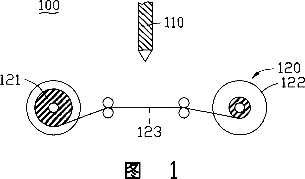
[0037] For the target product of the flexible circuit board, the holes on it are generally composed of copper holes formed on the copper film and film holes formed on the base film. The present invention relates to a device and method for forming film holes on the base film.

[0038] Please refer to FIG. 5 , which is a schematic cross-sectional structure diagram of the first flexible board to be etched in the present invention. The provided flexible board 300 to be etched includes a base film 310 and copper layers 320 on both sides of the base film 310 , and the base film 310 is polyimide or polyester. The surface of the copper layer 320 has a required copper hole 321 with a diameter of 0.05mm˜0.2mm, and the base film 310 is exposed outside at a position corresponding to the copper hole 321 . The bare base film 310 is the position where film holes are to be formed in the present invention, that is to say, the copper holes 321 can play a positioning role.

[0039] The copper h...


PUM


Abstract

A method for preparing pin hole on flexible circuit board includes providing flexible board to be etched and forming copper hole on said flexible board, exposing base diaphragm at position corresponding to said copper hole, sending flexible board into chemical etching system to finalize preparation of pin hole by conveying system on pin hole forming device. The pin hole forming device used for realizing said method is also disclosed.

Description

【Technical field】 [0001] The present invention relates to a method and device for manufacturing a flexible circuit board, in particular to a device and method for forming a film hole on a base film of a flexible circuit board. 【Background technique】 [0002] With the continuous development of science and technology, ultra-small mobile phones, portable calculators and automotive electronic products have put forward higher requirements for the miniaturization and light weight of products. In order to meet this demand, flexible printed circuit boards (Flexible Printed Circuit, abbreviated FPC, also known as soft boards, flexible circuit boards or flexible circuit boards) are gradually replacing them due to their thinness, toughness, flexibility, bendability and other excellent properties. The original rigid circuit board or circuit board module is more and more used in various electronic products. [0003] A conventional flexible circuit board includes a base film, conductive ...

Claims


Application Information

Patent Timeline
IPC IPC(8): H05K3/00H05K3/42H05K3/46
CPCH05K1/0393H01L21/67086H05K3/002H05K2203/1545
Inventor 许家硕
Owner AVARY HLDG (SHENZHEN) CO LTD
Learn More