
Marked electronic device shell

An electronic device and marking technology, applied in the direction of marking rigid planes, labels, packaging, etc., can solve the problems of reduced adhesive force, screw holes collapse, damage to the marking block or electronic device shell, etc., and achieve the effect of reducing production costs.

Inactive Publication Date: 2007-03-14
PEGATRON
View PDF0 Cites 9 Cited by
  • Summary
  • Abstract
  • Description
  • Claims
  • Application Information

AI Technical Summary

Problems solved by technology

In this way, the adhesive will be damaged, and the adhesive needs to be replaced
Furthermore, even if the back glue is not damaged, the adhesive force may be reduced due to rework, which will cause the marking block and the back glue to easily fall off from the electronic device casing in the future
[0006] In addition, the disadvantage of fixing the marking block on the housing of the electronic device by screw locking is that both the marking block and the electronic housing itself need to tap holes before the marking block can be fixed on the housing with screws
However, during the drilling process, both the marking block and the housing of the electronic device may not be able to lock the screw into the screw hole due to improper drilling.
In addition, in the operation of locking the marking block on the housing of the electronic device with screws, the screw hole may be broken due to improper operation, resulting in damage to the marking block or the housing of the electronic device

Method used


Image

  • Marked electronic device shell
  • Marked electronic device shell
  • Marked electronic device shell

Examples


Embodiment Construction

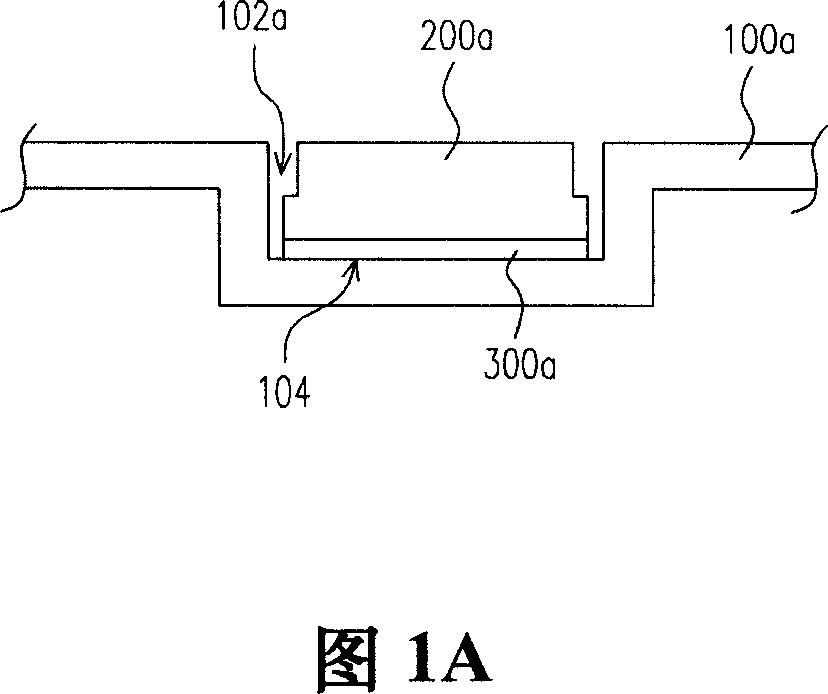
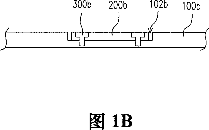
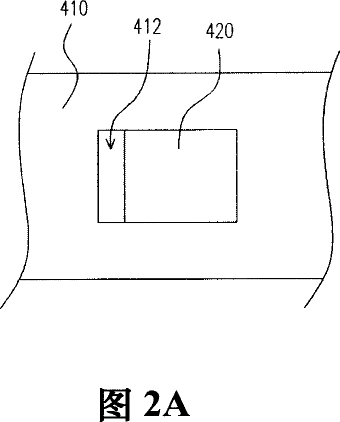
[0037] 2A is a top view of an electronic device housing according to a preferred embodiment of the present invention, FIG. 2B is a right side view of FIG. 2A , and FIG. 3 is a schematic diagram of a marking block fixed to an electronic device housing according to a preferred embodiment of the present invention. Please refer to FIG. 2A , FIG. 2B and FIG. 3 at the same time. The housing 400 of the electronic device with markings includes a housing board 410 , a carrying board 420 , a connecting board 430 and a marking block 440 . Wherein, the shell plate 410 has an opening 412 , and the carrying plate 420 is disposed below the opening 412 of the shell plate 410 . The connecting plate 430 is used for connecting one end of the supporting plate 420 to the shell plate 410 , and the connecting plate has an engaging hole 432 . In addition, the two sides of the marking block 440 have protruding parts 444a and 444b respectively, the protruding part 444b is used to be locked in the engag...


PUM


Abstract

This invention relates to electron device shell with label, which comprises open shell, load board, connection board and label block, wherein, the load board is down the shell open to connect to shell through card hole connection board; the label block is set on load board with protruding parts on both sides; one protruding part is used to set connection board card; the other protruding part is set down shell board to set the label card into open hole.

Description

technical field [0001] The present invention relates to a housing with markings, and more particularly to an electronic device housing with markings that are easy to rework. Background technique [0002] Today's general electronic products, such as desktop computers, notebook computers, handheld communication products, and various home appliances, etc., usually have identification marks (logo), such as model numbers or trademarks, on their casings. The existence of these identification marks can enable consumers to quickly identify the manufacturer and model of the product, so that consumers can judge the rough grade of the product quality accordingly. On the other hand, trademarks are also a useful tool for manufacturers to establish brand image, avoid counterfeiting and increase the added value of products. [0003] At present, one method of arranging the mark on the casing is to make the mark block with plastic material, and form a groove on the product shell by opening ...

Claims


Application Information

Patent Timeline
Patent Type & Authority Applications(China)
IPC IPC(8): H05K5/02B65C1/00
Inventor 张木财廖继诚
Owner PEGATRON
Learn More