


Quick Research
Generate reliable direction feasibility study reports for your R&D in just a few steps.

Technical Q&A
Discover and master advanced knowledge NOW. Basics, ideas, possibilities, all at once.

Find Solutions
As an expert in R&D theories, this can generate solutions to your technical problems instantly.

Evaluate Feasibility
Analyze your overall solution with one click, know your potential R&D risks in advance.

Monitor Landscape
Get weekly tech updates, stay abreast of the latest tech innovations and key insights.
Semiconductor device having a structure to improve contact processing margin, and method of fabricating the same
一种半导体、器件的技术,应用在结构的半导体器件及其制造领域,能够解决影响漏电流特性、半导体器件可靠性和良率下降等问题
- Summary
- Abstract
- Description
- Claims
- Application Information
AI Technical Summary
Problems solved by technology
Method used
Image

Examples
Embodiment Construction
[0021] specific implementation plan
[0022] In order to clarify the viewpoint of the present invention, technologies that are well known in the technical field and not directly related to the present invention are not described in this specification. For the same reason, some elements in the drawings are omitted, enlarged or approximated, and thus the size of the elements does not always reflect the actual situation.
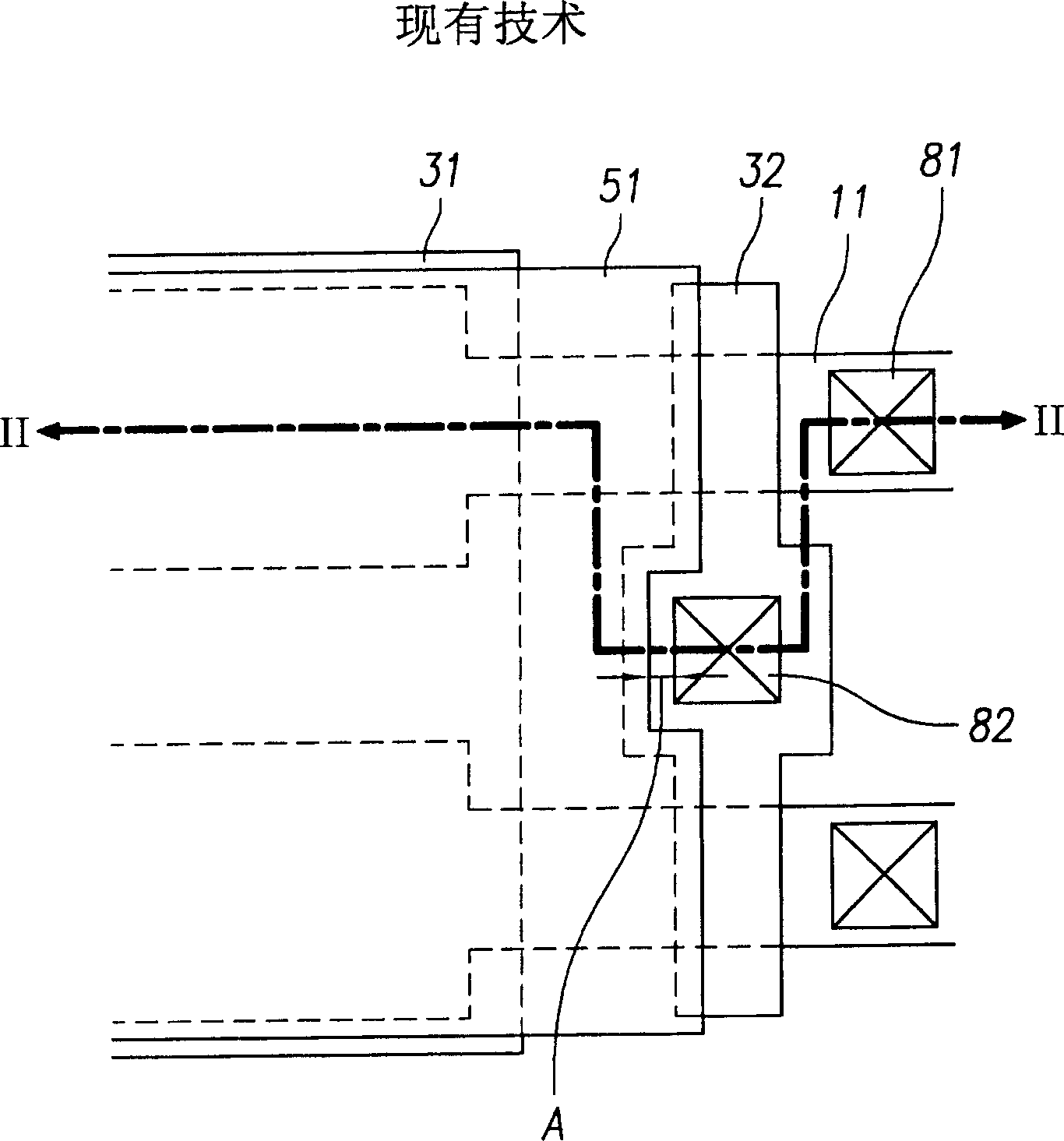
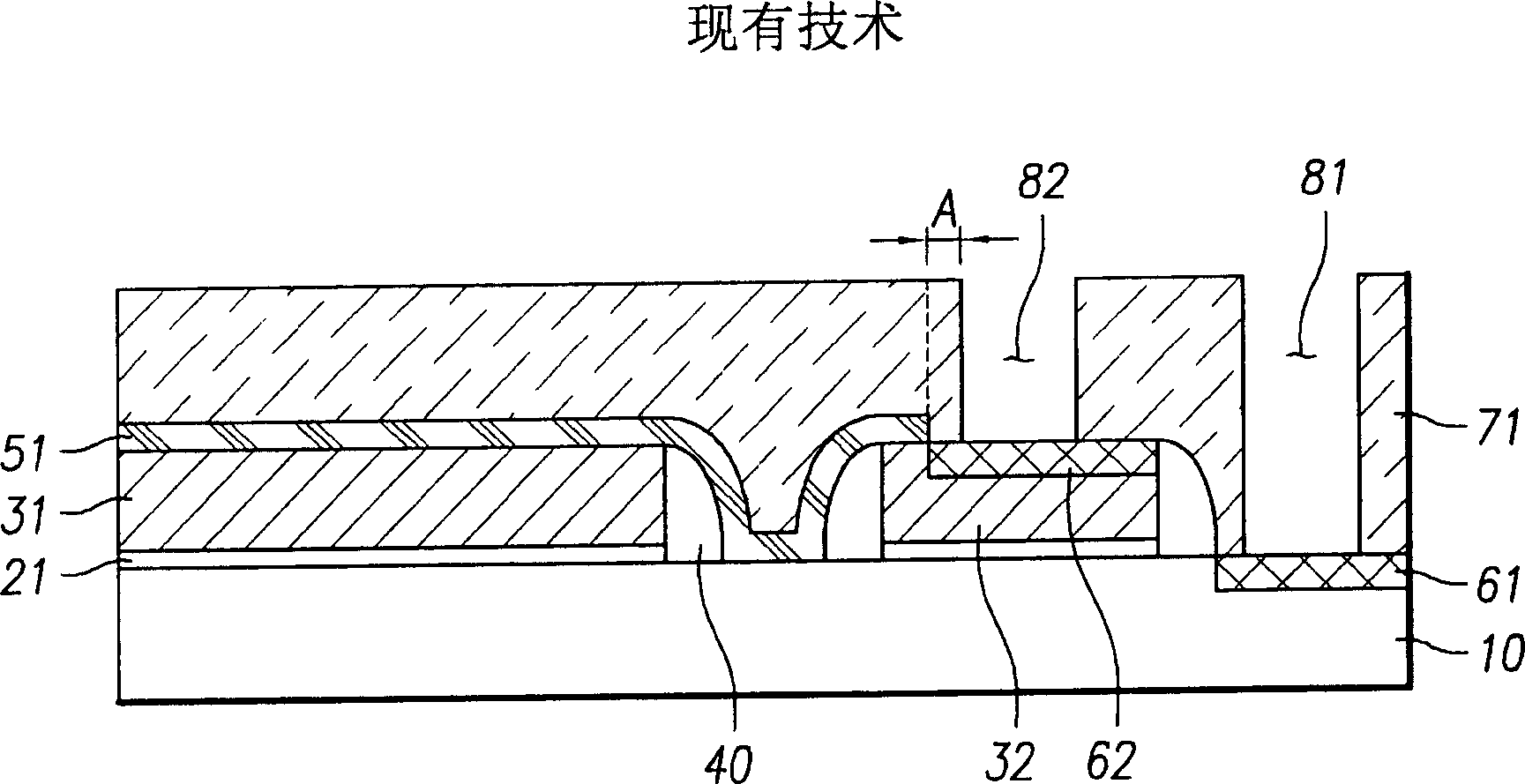
[0023] Figure 4 A partial design diagram showing a semiconductor device (IT-SRAM) according to an embodiment of the present invention. Figure 4 and figure 1 The basic design diagrams of semiconductor devices in are generic, such that they are used in Figure 4 The reference signs and figure 1 in the same. like Figure 4 As shown, the distance (B) between the non-salicide region 51 and the second contact 82 connected to the second conductive pattern 32 is sufficient for subsequent processing. In other words, a sufficient processing margin in the contact...
PUM
 Abstract
Description
Claims
Application Information
 - R&D Engineer
- R&D Manager
- IP Professional
- Industry Leading Data Capabilities
- Powerful AI technology
- Patent DNA Extraction
Browse by: Latest US Patents, China's latest patents, Technical Efficacy Thesaurus, Application Domain, Technology Topic, Popular Technical Reports.
© 2024 PatSnap. All rights reserved.Legal|Privacy policy|Modern Slavery Act Transparency Statement|Sitemap|About US| Contact US: help@patsnap.com