Semiconductor laser device and method for fabricating the same

A technology of laser device and semiconductor, applied in the direction of semiconductor laser device, semiconductor laser, laser device, etc., can solve the problem of laser emission stop and other problems

Inactive Publication Date: 2007-01-24
PANASONIC CORP
View PDF1 Cites 0 Cited by
  • Summary
  • Abstract
  • Description
  • Claims
  • Application Information

AI Technical Summary

Problems solved by technology

Due to the above, the temperature in the region near the emission edge surface of the active layer rises to the melting point of the crystals constituting each semiconductor layer, so that the part of the region near the emission edge surface of each semiconductor layer melts, causing the laser emission operation to stop.

Method used


Image

  • Semiconductor laser device and method for fabricating the same
  • Semiconductor laser device and method for fabricating the same
  • Semiconductor laser device and method for fabricating the same

Examples


no. 1 Embodiment

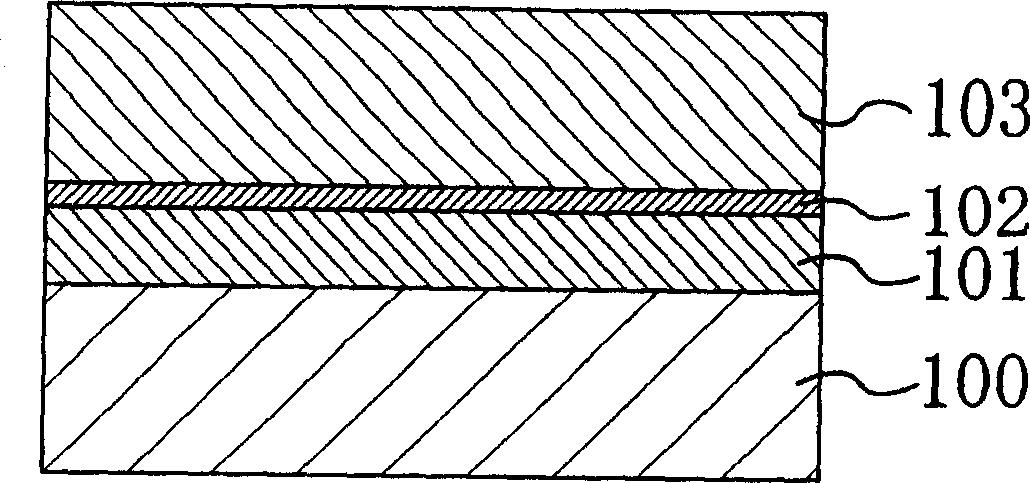
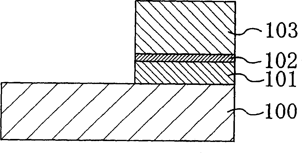
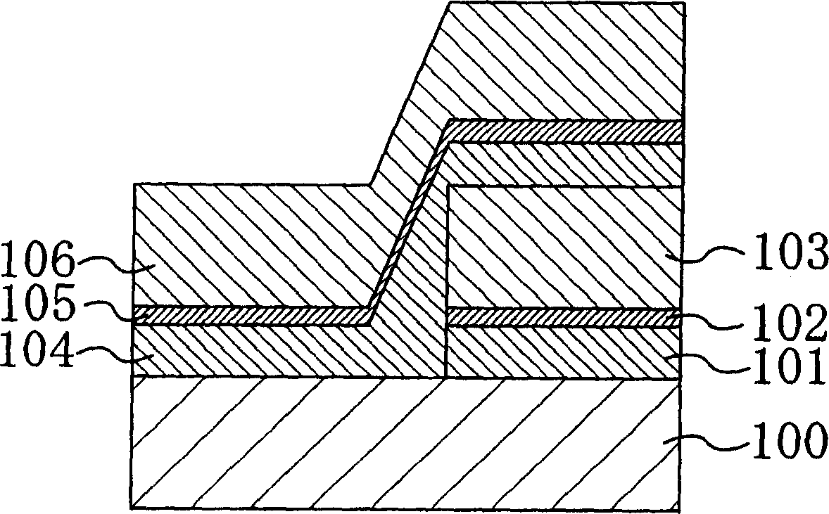
[0103] Below, refer to Figure 1(a) ~ Figure 1(d) , Figure 2(a) and Figure 2(b), and Figure 3(a) ~ Figure 3(d) , the method of manufacturing the semiconductor laser device according to the first embodiment of the present invention will be described.

[0104] Figure 1(a) ~ Figure 1(d) , Figure 2(a) and Figure 2(b), and Figure 3(a) ~ Figure 3(d) , is a sectional view showing a pivot portion step of the method of manufacturing the semiconductor laser device according to the first embodiment of the present invention.

[0105] here, Figure 1(a) ~ Figure 1(d) with Figure 3(a) ~ Figure 3(d) It is a cross-sectional view showing the pivotal part process of the manufacturing method of the semiconductor laser device, specifically, in Figure 4 The cross-sectional view of the pivotal part process of the line IIId-IIId shown, Fig. 2 (a) is the top view of the pivotal part process showing the manufacturing method of the semiconductor laser device, and Fig. 2 (b) is the manufacturing ...

no. 2 Embodiment

[0203] In the future, in response to higher-speed and multi-layer data writing such as DVD-RAM, the optical output required for semiconductor laser devices is 300 [mA] to 400 [mA], and higher output operations can be performed. Semiconductor laser devices will be required.

[0204] Therefore, the semiconductor laser device of the second embodiment of the present invention is not only the same as the aforementioned semiconductor laser device of the first embodiment of the present invention, but also has a good window area in the vicinity of the emission edge by a single Zn diffusion process. The purpose is to provide an infrared laser active layer and a red laser active layer in the region, and furthermore, to provide a semiconductor laser device capable of higher output operation.

[0205] Here, in order to realize a semiconductor laser device capable of higher output operation, it is necessary to inject more current into the active layer.

[0206] However, as the current inj...


PUM


Abstract

To provide a semiconductor laser, i.e. a monolithic integrated laser such as a two wavelength laser, having a good window region formed in each region near the exit end face of an active layer by single step for diffusing impurities, and to provide its fabrication process. The semiconductor laser comprises an element of first wavelength having a first conductivity type first clad layer, a first active layer having a first window region near the exit end face, and a second conductivity type first clad layer formed on a substrate sequentially in ascending order, and an element of second wavelength having a first conductivity type second clad layer, a second active layer having a second window region near the exit end face, and a second conductivity type second clad layer formed sequentially in ascending order. Lattice constants of the second conductivity type first clad layer and the second conductivity type second clad layer are constants adjusted to compensate for the difference in diffusion rate of impurities contained in the first window region of the first active layer and impurities contained in the second window region of the second active layer.

Description

technical field [0001] The present invention relates to semiconductor laser devices, in particular to DVD-RAM, DVD-R, DVD-RW, DVD+R, DVD+RW, CD-R, CD-RW, DVD-ROM, CD-ROM, DVD-Video Optical disc devices such as CD-DA and VCD, semiconductor laser devices used in information processing, optical communication, and optical measurement, and their manufacturing methods. Background technique [0002] Semiconductor laser devices are used as light sources for reading and writing of optical disc devices, and as light sources for optical information processing, optical communication, and optical measurement. For example, an AlGaInP-based red laser light with a wavelength of about 650 nm is used as a read / write light source for reading or writing to a DVD-RAM. Also, for example, an AlGaAs-based infrared laser with a wavelength of about 780 nm is used as a read / write light source for reading or writing a CD-R. [0003] In order to cope with both DVD-RAM and CD-R, one drive must have bot...

Claims


Application Information

Patent Timeline
Patent Type & Authority Applications(China)
IPC IPC(8): H01S5/40H01S5/026H01S5/323H01S5/343H01S5/16
CPCH01S5/1039H01S5/3211H01S5/4087H01S5/4031H01S5/34326H01S5/34313H01S5/3201H01S5/2231B82Y20/00H01S5/162
Inventor 福久敏哉万浓正也古川秀利
Owner PANASONIC CORP
Why Eureka
Try Eureka