Buffer circuit
A buffer circuit and power supply circuit technology, applied in the direction of logic circuit connection/interface layout, logic circuit coupling/interface using field effect transistors, reliability improvement and modification, etc., can solve the operation speed limit, PMOS transistor signal rising slowly, semiconductor Increased device size, etc.
- Summary
- Abstract
- Description
- Claims
- Application Information
AI Technical Summary
Problems solved by technology
Method used
Image

Examples
no. 1 example
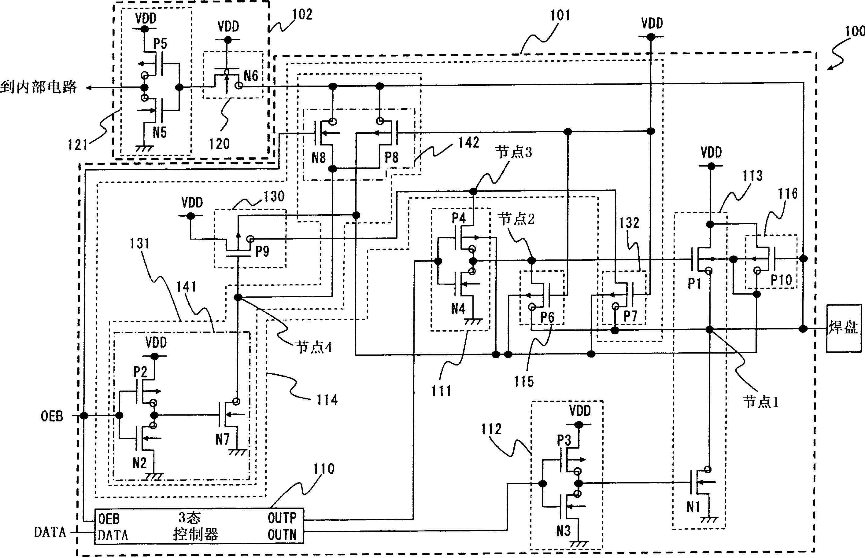
[0028] figure 1 A buffer circuit 100 according to a first embodiment of the present invention is shown. Refer below figure 1 The buffer circuit 100 will be specifically described. The buffer circuit 100 uses one input / output (I / O) terminal in an input mode and an output mode. The I / O terminal of the buffer circuit is connected to, for example, an I / O terminal of a semiconductor device. The buffer circuit includes an output buffer 101 used in an output mode and an input buffer 102 used in an input mode. The output buffer 101 outputs a signal DATA, which is supplied from an internal circuit to an I / O terminal, during an output mode. The input buffer 102 outputs the signal input to the input / output circuit to the internal circuit. The output mode and the input mode are switched by the OEB signal input to the buffer circuit 100 from the internal circuit. If the OEB signal is at a low level (such as ground voltage GND), the buffer circuit 100 enters an output mode; if the OEB...
no. 2 example
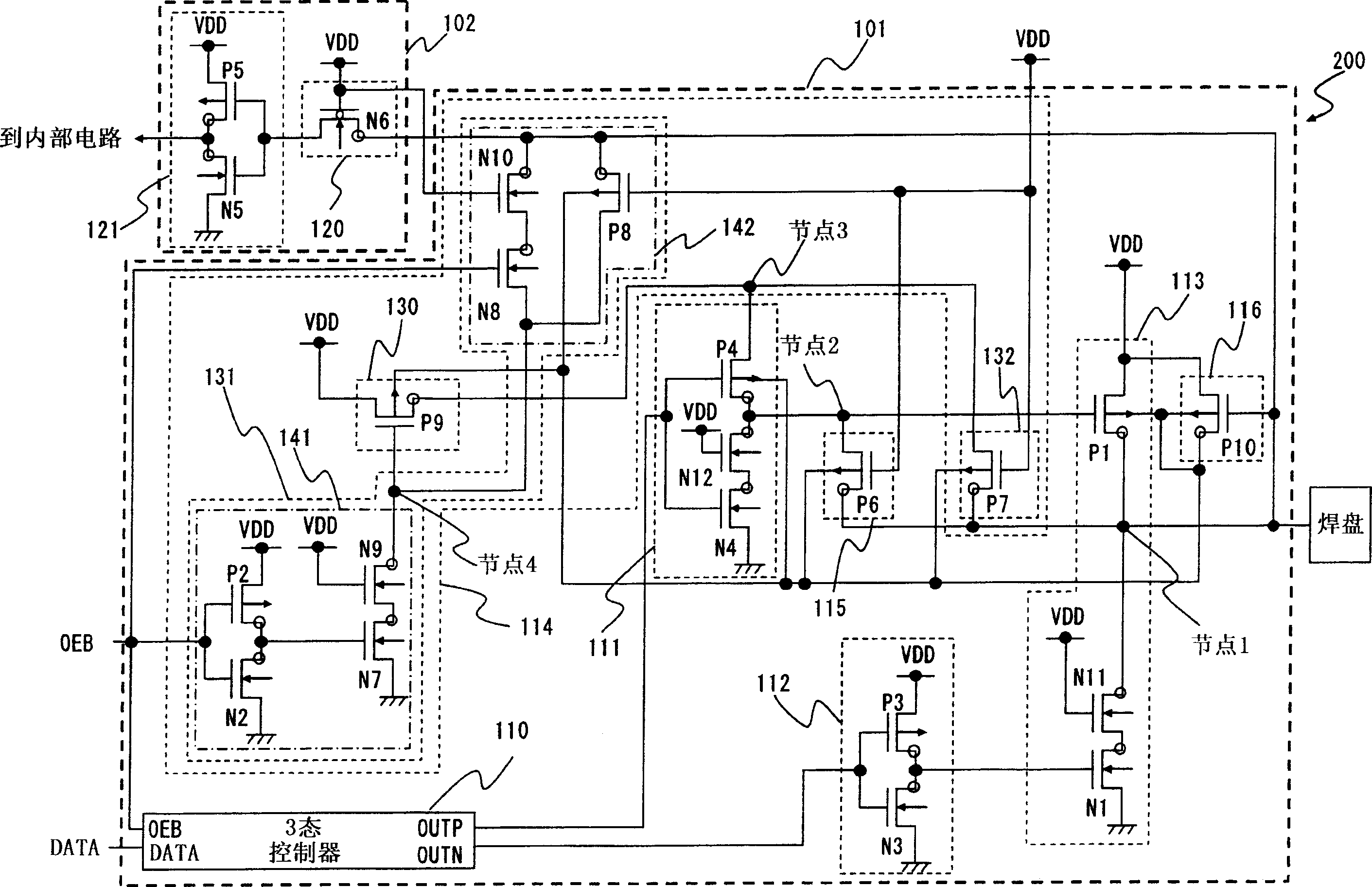
[0078] Image 6 is a circuit diagram of a buffer circuit 600 according to a second embodiment of the present invention. The buffer circuit 600 of the second embodiment is basically the same circuit as the buffer circuit 100 of the first embodiment. The buffer circuit 600 of the second embodiment differs from the buffer circuit 100 of the first embodiment in the connection of the gate of the PMOS transistor P10 in the N-well controller 116 . The same elements as those of the buffer circuit 100 of the first embodiment are denoted by the same reference numerals and will not be described in detail here.
[0079] The gate of the PMOS transistor P10 in the buffer circuit 100 of the first embodiment is connected to the I / O terminal. In the buffer circuit 600 of the second embodiment, the gate of the PMOS transistor P10 is connected to a line connecting the NMOS transistor N7 and the PMOS transistor P9 of the power supply circuit 114 .
[0080] In this connection, the N-well contro...
no. 3 example
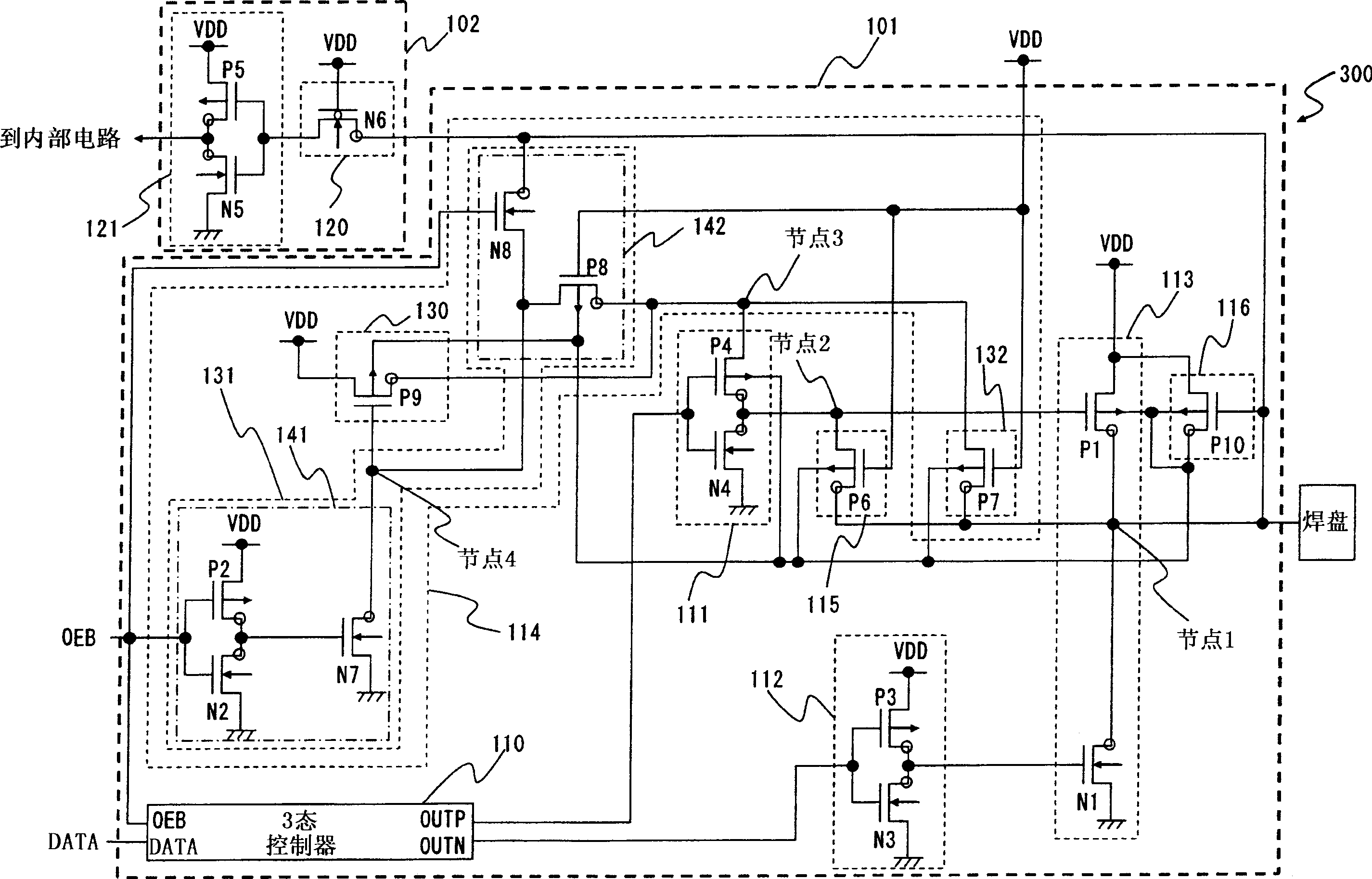
[0086] Figure 9 is a circuit diagram of a buffer circuit 900 according to a third embodiment of the present invention. The buffer circuit 900 of the third embodiment is basically the same circuit as the buffer circuit 100 of the first embodiment. The buffer circuit 900 of the third embodiment differs from the buffer circuit 100 of the first embodiment only in that the PMOS transistor P7 is omitted. The same elements as those of the buffer circuit 100 of the first embodiment are denoted by the same reference numerals and will not be described in detail here.
[0087] The buffer circuit 900 of the third embodiment does not have the PMOS transistor P7. However, when an external power supply voltage is input to the I / O terminal, the external power supply voltage is supplied to the gate of the PMOS transistor P9 through the NMOS transistor N8 and the PMOS transistor P8. Therefore, since the connection between the pre-driver 111 and the power supply voltage VDD is blocked, curre...
PUM
 Abstract
Description
Claims
Application Information
 - R&D
- Intellectual Property
- Life Sciences
- Materials
- Tech Scout
- Unparalleled Data Quality
- Higher Quality Content
- 60% Fewer Hallucinations
Browse by: Latest US Patents, China's latest patents, Technical Efficacy Thesaurus, Application Domain, Technology Topic, Popular Technical Reports.
© 2025 PatSnap. All rights reserved.Legal|Privacy policy|Modern Slavery Act Transparency Statement|Sitemap|About US| Contact US: help@patsnap.com