High-tension element structure

A technology of high-voltage components and conductivity types, applied in the field of high-voltage component structures that can suppress parasitic currents, can solve problems such as unpredictable output current and voltage characteristics, and achieve the effect of being conducive to small size and suppressing parasitic currents

Active Publication Date: 2006-09-13
UNITED MICROELECTRONICS CORP
View PDF0 Cites 0 Cited by
  • Summary
  • Abstract
  • Description
  • Claims
  • Application Information

AI Technical Summary

Problems solved by technology

However, the size of the current device is shrinking and shrinking, causing the channel diffusion region 16 to be longer than the source diffusion region 20 and the drain diffusion region 22. The protruding regions 36 and 38 have a high gate voltage and generate a lot of parasitic currents (parasitical current), And cause unpredictable output current voltage characteristic (I-V characteristic) curve

Method used


Image

  • High-tension element structure
  • High-tension element structure
  • High-tension element structure

Examples


Embodiment Construction

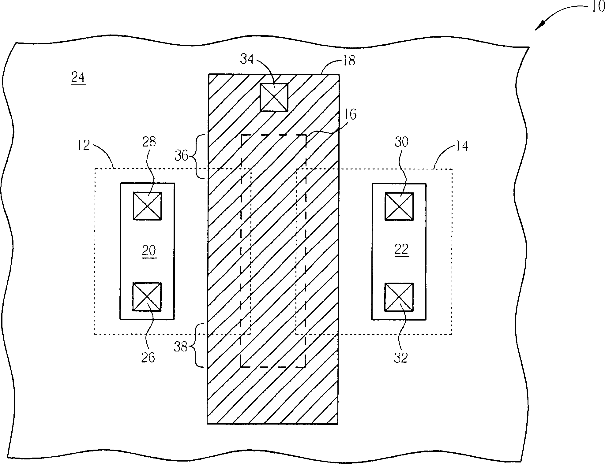
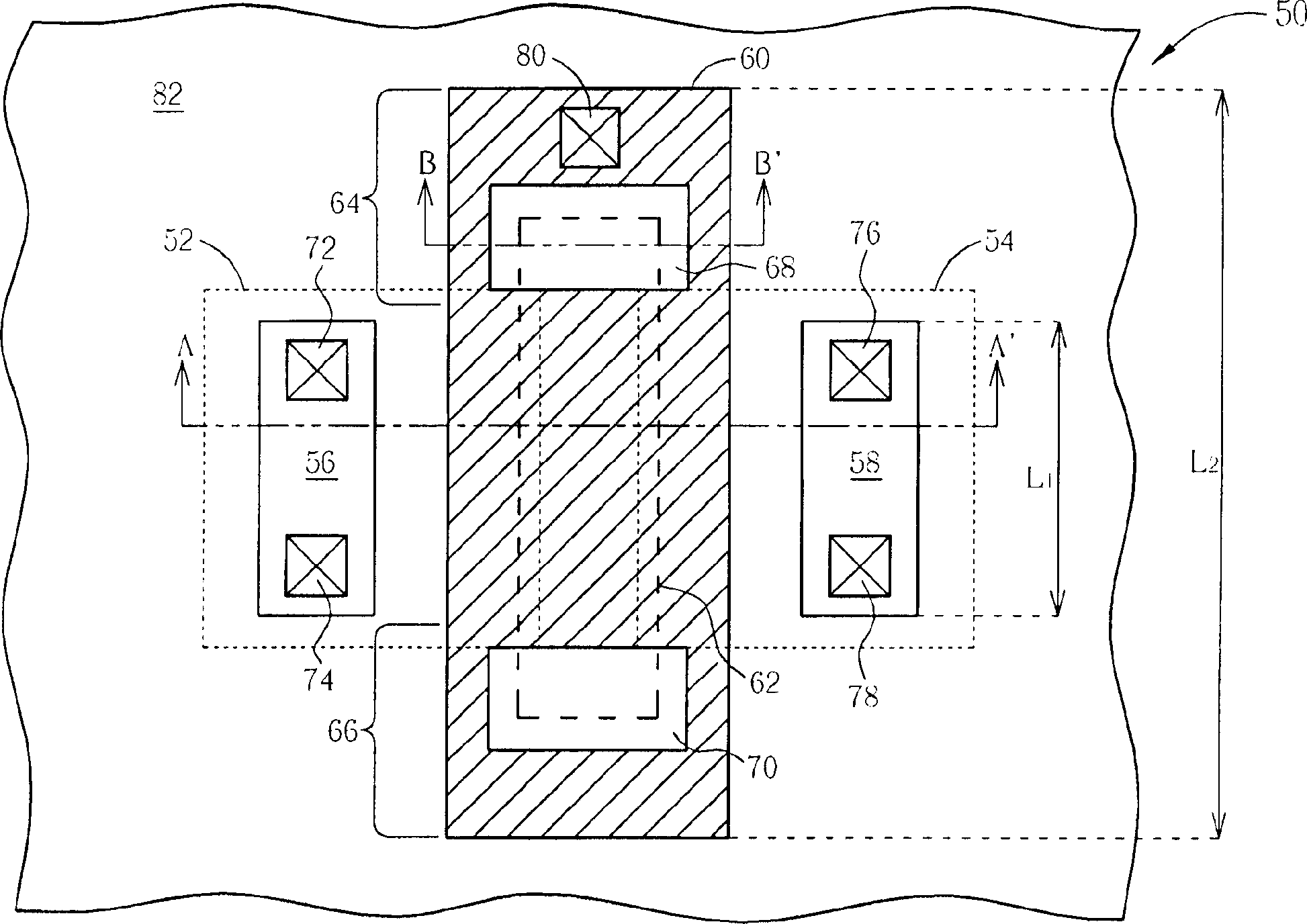
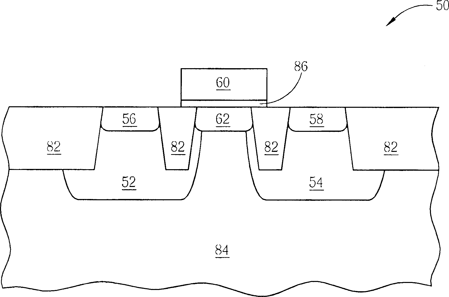
[0031] Please refer to figure 2 , figure 2 It is a top view of the high voltage element structure 50 of the present invention. like figure 2 As shown, the high-voltage element structure 50 of the present invention is disposed in a substrate (not shown) of a first conductivity type, and the high-voltage element structure includes a first well region 52 (shown by a dotted line) having a second conductivity type region) and a second well region 54 (the region shown by the dotted line) are located in the substrate and have a first length L 1 A source diffusion region 56 and a drain diffusion region 58 are respectively located in the first well region 52 and the second well region 54, and have a second length L 2 A conductive gate layer 60 is located on the surface of the substrate, and a channel diffusion region 62 (the region shown by the dotted line) is located in the substrate covered by the conductive gate layer 60 and is located above part of the first well region 52 an...


PUM


Abstract

A high voltage element structure is set in a base of a first conduction kind, a first well region and a second well region with a second conduction kind are set in the base, a source diffusion region and a drain diffusion region with a first length are placed in the first and second well regions and a conductor grating layer with a second length is place on the surface of the base, in which, the second length is greater than the first, thus two projecting regions form at both sides of the conductor grating layer and two windows are set at the projecting regions separately.

Description

technical field [0001] The invention relates to a high-voltage component structure, in particular to a high-voltage component structure capable of suppressing parasitic current. Background technique [0002] In recent years, with the vigorous development of electronic communication products such as mobile phones, the drivers for liquid crystal displays (LCDs) used therein are particularly important. Today, the industry has developed products with 32 volts and 0.18 micron high-voltage technology to be used in portable single-chip thin film transistor liquid crystal display (thin film transistor liquid crystal display; TFT LCD) and other fields. The feature of this technology is that it can be used for Different voltages are provided for the gate drive, source drive and controller, enabling it to be embedded in ultra-high density static random access memory (SRAM) devices and to produce smaller chips. [0003] Please refer to figure 1 , figure 1 It is a top view of the exis...

Claims


Application Information

Patent Timeline
Patent Type & Authority Applications(China)
IPC IPC(8): H01L29/78
Inventor 李文芳徐尉伦林育贤
Owner UNITED MICROELECTRONICS CORP
Why Eureka
Try Eureka