Optical element, optical system and manufacture method thereof, optical device
A technology for optical components and manufacturing methods, applied in the directions of optical components, optical components, optics, etc., can solve problems such as difficulty in securing space, and achieve the effect of simple setting of marks, easy positioning and assembly
- Summary
- Abstract
- Description
- Claims
- Application Information
AI Technical Summary
Problems solved by technology
Method used
Image


Examples
Embodiment 1
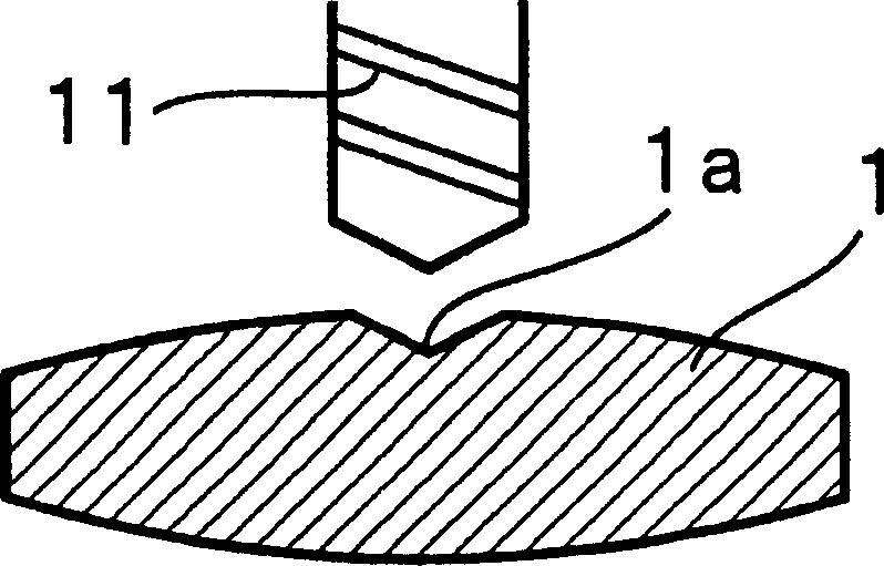
[0073] figure 1 It is a side view which shows the lens which is an optical element which is one Example of this invention. Such as figure 1 As shown, a mark 1a formed of a concave portion is formed at the center of the lens 1 . Such as figure 1 As shown, the circular mark 1a composed of a concave portion can be formed by a cutting tool 11 such as a drill. The lens 1 is made of BK7 glass, the lens diameter is 3 mm, and the diameter of the mark 1a is 200 μm. In addition, the depth of the mark 1a is about 50 μm.
[0074] In addition, in this embodiment, as a lens that can be used in a digital camera with 8-bit grayscale, since the area of the mark 1a is set to 0.4% of the effective optical surface of the lens, the shape of the mark is circular, so the mark's The effective size, that is, the diameter, is 200 μm. However, when the lens is smaller than the lens of this embodiment, when it is used in a digital device with a higher number of digits, or in a device with a large...
Embodiment 2
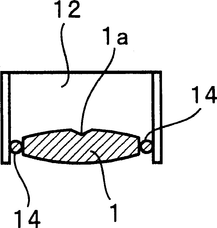
[0076] Figure 2 ~ Figure 4 is said to be figure 1 A diagram of the process of manufacturing an optical system by combining the lens shown in and other components. Lens 1, used as in image 3 It is fixed by the semi-cylindrical frame 12 and frame 13 as shown in the perspective view.
[0077] First, if figure 2 As shown, the lens 1 is attached to the inside of the semi-cylindrical frame 12 using an adhesive 14 .
[0078] Next, if Figure 4 As shown in (a), the lens 1 attached to the semi-cylindrical frame 12 is arranged at the focal point position below the microscope 14 . In this state, the lens 1 is moved in the horizontal direction so that the mark 1 a of the lens 1 is located at the position of the scale 14 a within the field of view of the microscope 14 .
[0079] Next, if Figure 4 As shown in (b), the semi-cylindrical frame 12 and the lens 1 are moved downward by a predetermined amount based on the lens design, as shown in Figure 4 As shown in (c), the lens 15,...
Embodiment 3
[0085] Figure 5 It is a camera module representing an optical device that is assembled as an optical system formed by the lens 1 and the lens 15 mounted on the frames 12 and 13 as described above, mounted on the imaging element (CCD) 17 provided in the barrel 16 sectional view.
[0086] in as Figure 5 In the camera module of the optical device shown in , the positioning of the imaging element and the optical system can be performed in the same manner as described in the second embodiment. In this case, it is desirable to provide a mark also on the imaging element, but since a pixel pattern is already formed in a CCD or the like, this pixel pattern can be used as a mark. In this embodiment, there is no need to specially provide marks on the imaging element, and the positioning of the imaging element and the optical system is performed using the pixel pattern of the imaging element as a reference.
[0087] Figure 24 is used Figure 5 A block diagram of a digital camera d...
PUM
| Property | Measurement | Unit |
|---|---|---|
| diameter | aaaaa | aaaaa |
| diameter | aaaaa | aaaaa |
Abstract
Description
Claims
Application Information
 - Generate Ideas
- Intellectual Property
- Life Sciences
- Materials
- Tech Scout
- Unparalleled Data Quality
- Higher Quality Content
- 60% Fewer Hallucinations
Browse by: Latest US Patents, China's latest patents, Technical Efficacy Thesaurus, Application Domain, Technology Topic, Popular Technical Reports.
© 2025 PatSnap. All rights reserved.Legal|Privacy policy|Modern Slavery Act Transparency Statement|Sitemap|About US| Contact US: help@patsnap.com