Plasma display panel and method producing same

A display panel, plasma technology, applied in the direction of alternating current plasma display panel, cold cathode manufacturing, electrode system manufacturing, etc., can solve the problems of increased processing time, increased manufacturing cost, decreased productivity, etc., to prevent alignment errors, improve productivity, The effect of reducing manufacturing costs

Inactive Publication Date: 2006-08-09
LG ELECTRONICS INC
View PDF0 Cites 0 Cited by
  • Summary
  • Abstract
  • Description
  • Claims
  • Application Information

AI Technical Summary

Problems solved by technology

[0015] In the process of manufacturing the front panel of the PDP, printing, drying, and photolithography are repeatedly performed, which increases the processing time, reduces the productivity, and increases the manufacturing cost
Also, an alignment error occurs between the black layer 104 formed on the transparent electrode and the bus electrode 102

Method used


Image

  • Plasma display panel and method producing same
  • Plasma display panel and method producing same
  • Plasma display panel and method producing same

Examples


no. 1 example

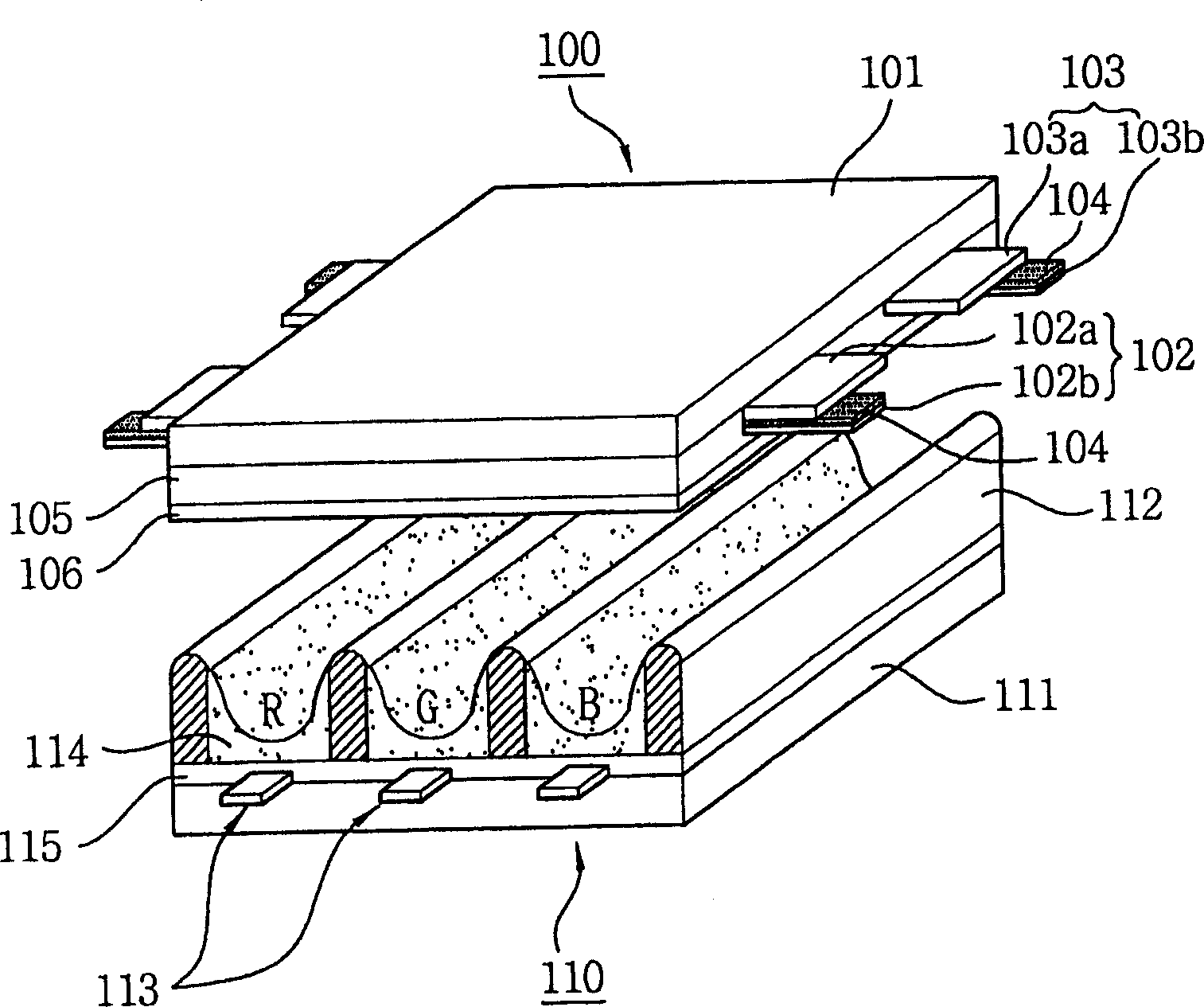
[0042] image 3 The structure of the PDP according to the first embodiment of the present invention is illustrated.

[0043] refer to image 3 , in the PDP according to the first embodiment of the present invention, the front panel 300 and the rear panel 310 are combined with each other and run parallel to each other at uniform intervals, wherein by arranging a plurality of pairs of scan electrodes 302 and sustain electrodes 303 The front panel 300 is obtained by sustain electrode pairs, and the rear panel 310 is obtained by arranging a plurality of address electrodes 313 to cross the plurality of sustain electrode pairs.

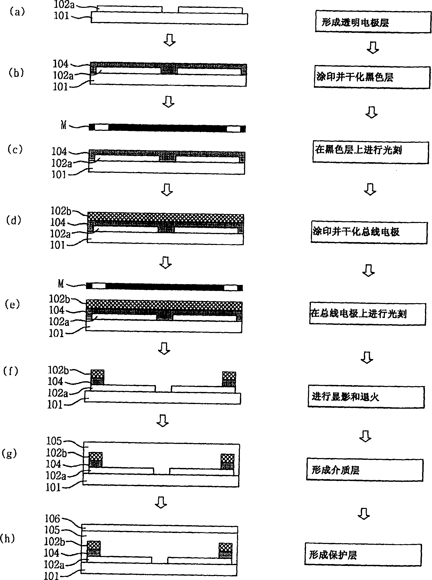
[0044] In the front panel 300, a scan electrode 302 and a sustain electrode 303 are formed on a front glass 301, which are used to mutually discharge within one cell to sustain emission of the cell. The scan electrodes 302 and the sustain electrodes 303 include transparent electrodes 302a and 303a made of a transparent material, and bus electrodes 302b an...

no. 2 example

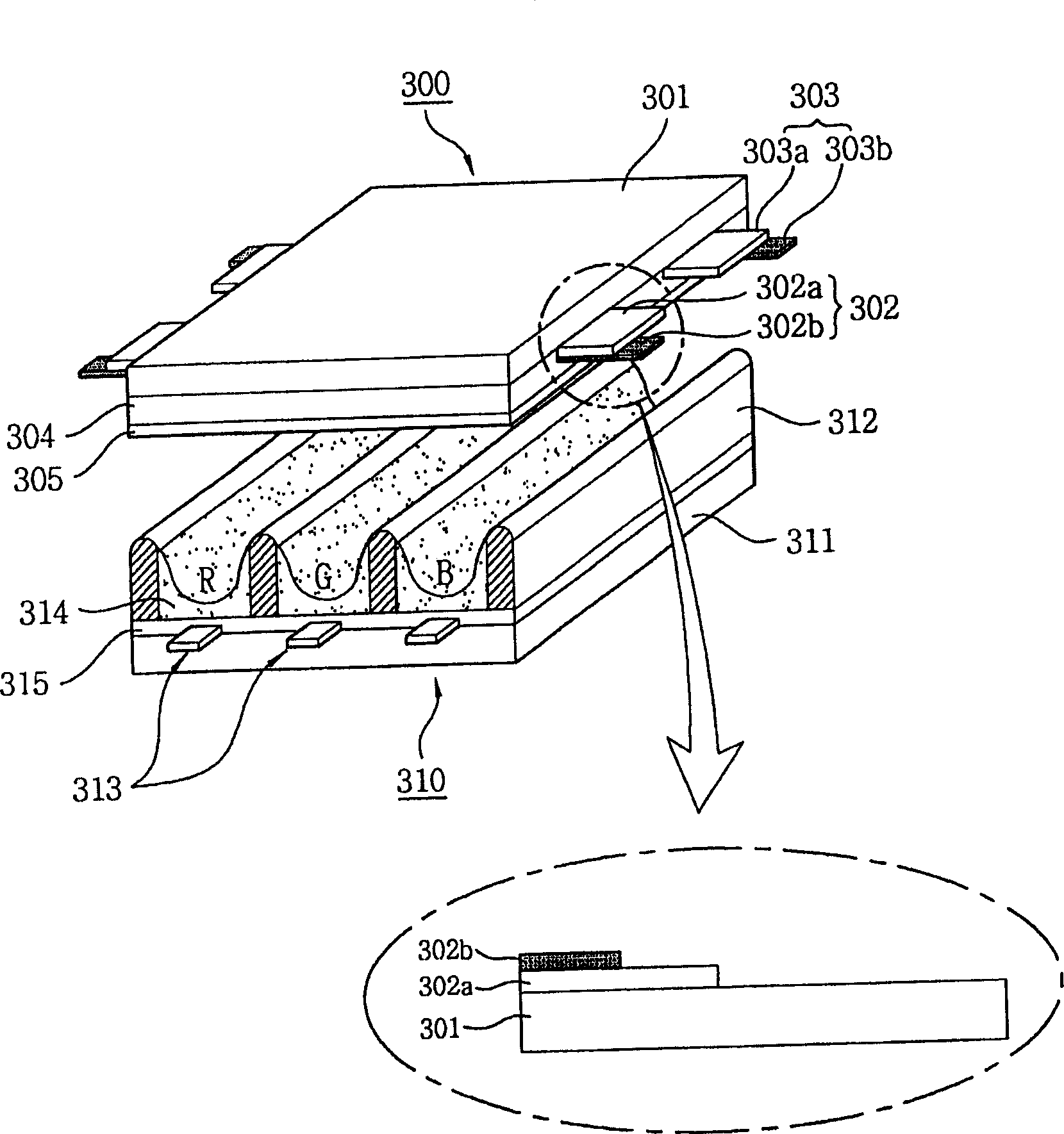
[0072] Figure 6 The structure of the PDP according to the second embodiment of the present invention is illustrated.

[0073] refer to Figure 6 , the structure of the PDP according to the second embodiment of the present invention is almost the same as that according to the first embodiment of the present invention. Therefore, a description of its structure which is the same as that of the PDP according to the first embodiment of the present invention will be omitted. In the PDP according to the second embodiment of the present invention, scan electrodes 402 and sustain electrodes 403 do not include transparent electrodes but include only bus electrodes 402b and 403b.


PUM


Abstract

A plasma display panel (PDP) and a method of manufacturing the same are provided. The PDP comprises a front panel (101) in which bus electrodes (102b,103b) comprising a black material (104) are formed on transparent electrodes (102a,103a) and a rear panel (111) attached to the front panel (101) to be separated from each other by a predetermined distance.

Description

technical field [0001] The present invention relates to a plasma display device, and more particularly, to a plasma display panel (PDP) and a manufacturing method thereof. Background technique [0002] In a plasma display panel (PDP), a main discharge gas such as Ne, He, and Ne+He and an inert gas including a small amount of xenon are injected into a discharge space between a front panel and a rear panel. When a discharge is generated by a high-frequency voltage, an inert gas in the discharge space generates vacuum ultraviolet (UV) rays, and the vacuum UV rays emit light through the phosphor, thereby realizing an image. [0003] figure 1 The structure of a typical PDP is illustrated. [0004] Such as figure 1 As shown, according to the PDP, the front panel 100 and the rear surface 110 are combined parallel to each other at uniform intervals, wherein the front panel 100 is obtained by arranging a pair of sustain electrodes formed by paired scan electrodes 102 and sustain e...

Claims


Application Information

Patent Timeline
Patent Type & Authority Applications(China)
IPC IPC(8): H01J17/49H01J17/04H01J17/02H01J9/02H01J11/12H01J11/22H01J11/24H01J11/26H01J11/34H01J11/36H01J11/38H01J11/42H01J11/44H01J11/50
CPCH01J11/24H01J2211/225H01B1/22H01J2211/444H01J9/02H01J11/12A41C3/065A41C3/122A41C3/0007
Inventor 张铭洙
Owner LG ELECTRONICS INC
Why Eureka
Try Eureka