
Image display device and method of manufacturing the same

A technology of image display device and manufacturing method, which is applied to image/graphic display tubes, identification devices, lighting devices, etc., and can solve problems such as incomplete packaging, leakage, and impairment of performance and life of display devices

Inactive Publication Date: 2006-07-05
KK TOSHIBA
View PDF1 Cites 9 Cited by
  • Summary
  • Abstract
  • Description
  • Claims
  • Application Information

AI Technical Summary

Problems solved by technology

However, in the case of using a metal frame, if the affinity between the metal frame and the sealing material is poor, it is difficult to securely seal the substrates together
As a result, the encapsulation is not complete and leakage may occur
If the sealing part leaks, it is difficult to maintain a high vacuum inside the case, thereby degrading the performance and life of the display device

Method used


Image

  • Image display device and method of manufacturing the same
  • Image display device and method of manufacturing the same
  • Image display device and method of manufacturing the same

Examples


Embodiment Construction

[0026] Embodiments in which an image display device according to the present invention is applied to an FED will now be described in detail with reference to the accompanying drawings.

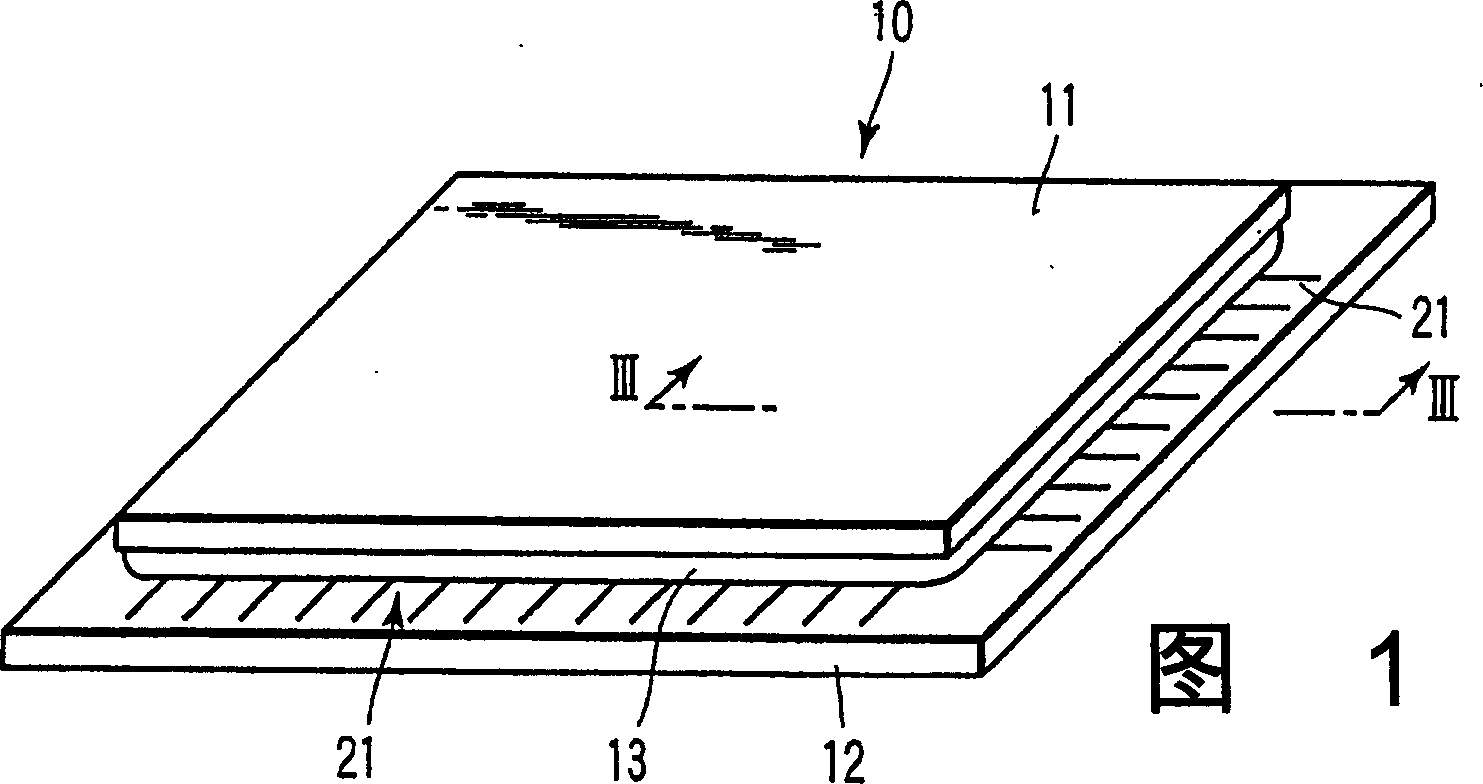
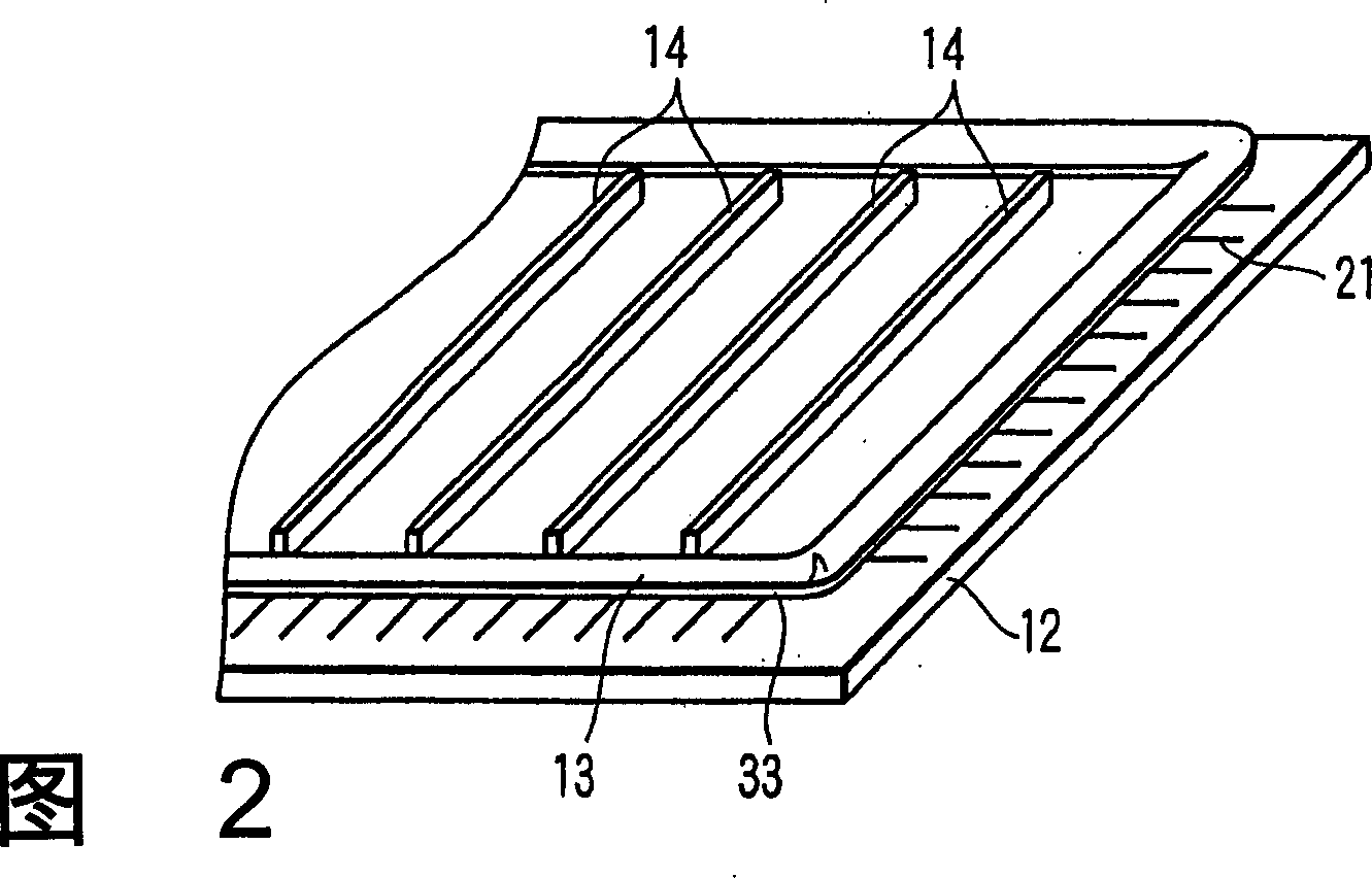
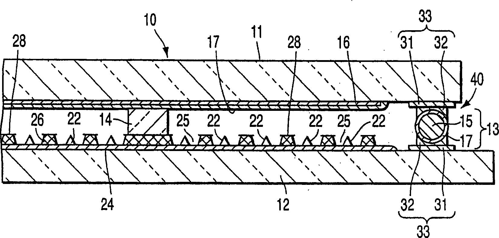
[0027] As shown in FIGS. 1 to 3, the FED includes a front substrate 11 and a back substrate 12 each composed of a rectangular glass plate as an insulating substrate. These substrates are placed facing each other with a gap of about 1.5 to 3 mm between them. The front substrate 11 and the back substrate 12 have their peripheral edge portions joined together by side walls 13 in the form of rectangular frames, thereby forming a planar rectangular enclosure 10, the inside of which is kept vacuum.

[0028] The respective peripheral edge portions of the front substrate 11 and the back substrate 12 are bonded together by the sealing portion 40 . In particular, the side wall 13 functioning as a frame is located between the sealing surface on the peripheral edge portion on the inner surface of the fro...


PUM

PropertyMeasurementUnit
thicknessaaaaaaaaaa
melting pointaaaaaaaaaa

Abstract

A vacuum envelope (10) of an image display comprises a front plate (11) and a back plate (12) arranged opposite to each other and a seal portion (40) by which the peripheral portion of the front plate and that of the back plate are sealed with each other. The seal portion comprises a frame body (13) lying along the peripheral portions of the front and back plates and a sealing material (32). The frame body has a core member (15) made of a metal and a metal coating (17) covering the surface of the core member.

Description

technical field [0001] The present invention relates to a flat image display device having opposing substrates and a large number of electron-emitting elements located inside one of the substrates, and also to a method of manufacturing the display device. Background technique [0002] In recent years, various flat display devices have been developed as next-generation lightweight, thin display devices to replace cathode ray tubes (CRTs). These flat display devices include liquid crystal display devices (LCDs), plasma display devices (PDP), field emission display devices (FEDs), surface conduction electron emission display devices (SEDs), and the like. In LCDs, the orientation of liquid crystals is used to control the intensity of light. In a PDP, phosphor emission is caused by ultraviolet rays generated by plasma discharge. In FEDs, phosphor emission is caused by electron beams from field emission electron emission elements. SED is a type of FED, a...

Claims


Application Information

Patent Timeline
Patent Type & Authority Applications(China)
IPC IPC(8): H01J29/86H01J9/26H01J31/12H05B33/04G09F9/30H01J9/40H01L51/50H05B33/14
CPCH01J31/127H01J29/86H01J9/261B65H2301/46011H01J1/30
Inventor 山田晃义海野洋敬
Owner KK TOSHIBA
Learn More