DC bias cancel circuit
一种消除电路、直流偏压的技术,应用在负反馈电路布置、电气元件、带有半导体器件/放电管的放大器等方向,能够解决高功率耗损、电路面积过大等问题
- Summary
- Abstract
- Description
- Claims
- Application Information
AI Technical Summary
Problems solved by technology
Method used
Image
Examples
Embodiment Construction
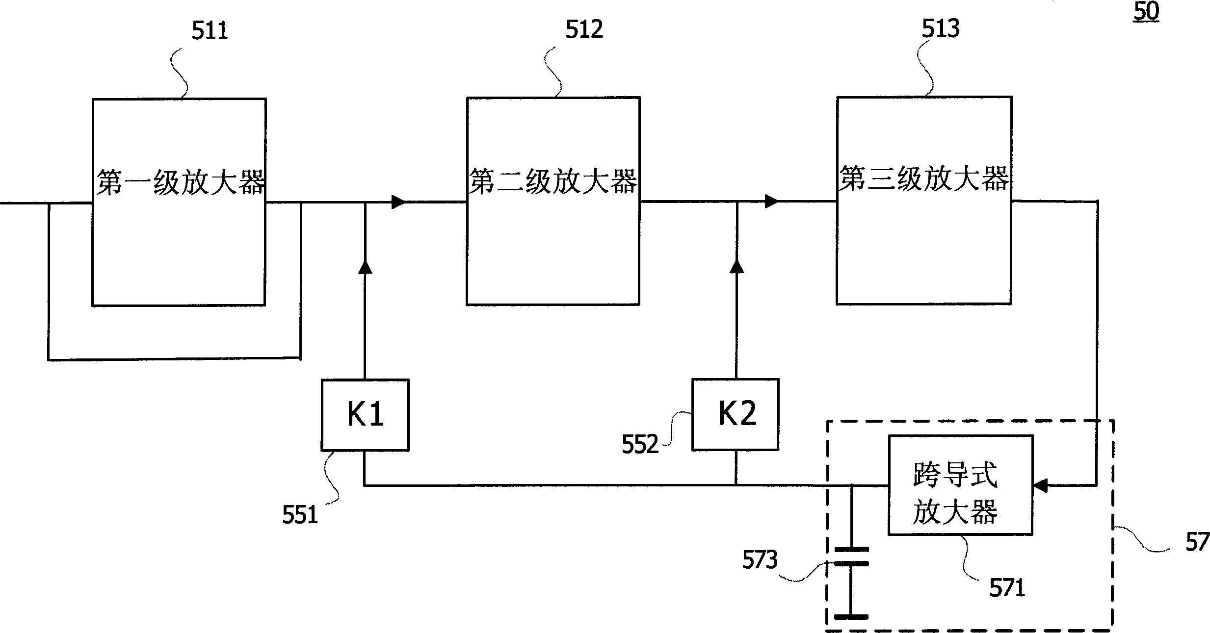
[0049] First, please refer to image 3 , is a block diagram of a preferred embodiment of the present invention. As shown in the figure, taking the use of three-stage amplifiers as an example, the DC bias elimination circuit 50 of the present invention mainly includes: a first-stage amplifier 511 , a second-stage amplifier 512 and a third-stage amplifier 513 . The amplifiers 511, 512 and 513 of each stage are negatively connected to a variable bandwidth switch respectively.
[0050] The DC bias cancellation circuit 50 has two variable gain amplifiers 551 and 552 . Wherein, the output terminal of the first variable gain amplifier 551 is connected to the series connection between the first stage amplifier 511 and the second stage amplifier 512; the output terminal of the second variable gain amplifier 552 is connected to the second stage amplifier 512 and the second stage amplifier 512. The series connection between the third stage amplifier 513 . The variable gain amplifiers ...
PUM
 Abstract
Description
Claims
Application Information
 - R&D
- Intellectual Property
- Life Sciences
- Materials
- Tech Scout
- Unparalleled Data Quality
- Higher Quality Content
- 60% Fewer Hallucinations
Browse by: Latest US Patents, China's latest patents, Technical Efficacy Thesaurus, Application Domain, Technology Topic, Popular Technical Reports.
© 2025 PatSnap. All rights reserved.Legal|Privacy policy|Modern Slavery Act Transparency Statement|Sitemap|About US| Contact US: help@patsnap.com


