
Output stage structure

An output stage, metal technology, applied in the field of complementary metal oxide semiconductor transistor output stage structure, can solve the problem that the bias voltage cannot be controlled independently

Active Publication Date: 2013-01-30
REALTEK SEMICON CORP
View PDF4 Cites 0 Cited by
  • Summary
  • Abstract
  • Description
  • Claims
  • Application Information

AI Technical Summary

Problems solved by technology

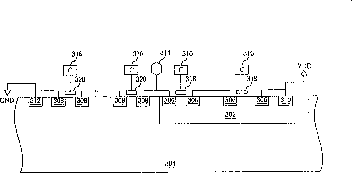
[0006] figure 2 Since all PMOSs share the same n-type well 302 and all NMOSs share the same p-type substrate 304, it is impossible to control the bias voltage independently for the substrate terminal of a single NMOS or PMOS.

Method used


Image

  • Output stage structure
  • Output stage structure
  • Output stage structure

Examples


Embodiment Construction

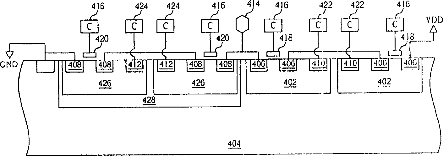
[0031] In the embodiment of the present invention, the high withstand voltage output stage is manufactured with a twin well (Twin well) process, so each NMOS transistor or PMOS transistor element has its own separate well area (Well), and users can Bias voltages are applied to the terminals of the substrate respectively, so that the voltage difference on the junction in the well region can be controlled to be reduced, so that the overall output stage is no longer limited by the junction breakdown voltage.

[0032] Please refer to image 3 , image 3 It is a schematic cross-sectional view of a high withstand voltage output stage structure according to an embodiment of the present invention. image 3As shown in FIG. 2 , a plurality of NMOS transistor elements and a plurality of PMOS transistor elements are fabricated on a p-type substrate (p substrate) 404 in a double well process. There are a plurality of separate n-type wells (n wells) 402 on the p-type substrate 404, and tw...


PUM


Abstract

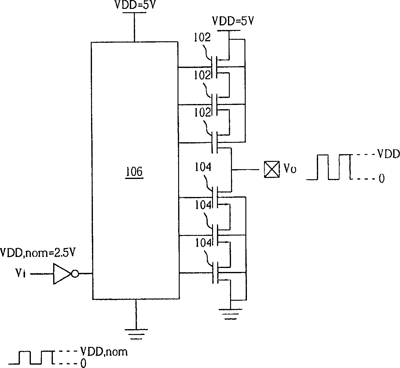
The invention relates to an output stage structure, which includes first and second p-type MOS transistors and first and second n-type MOS transistors, wherein the MOS transistors are made by double-well technology. The source of the first p-type MOS transistor is connected to the voltage source, and the gate is connected to the first voltage; the source of the second p-type MOS transistor is connected to the drain of the first p-type MOS transistor, the gate is connected to the second voltage, and the drain is connected to the second voltage. output pad; the drain of the first n-type MOS transistor is connected to the output pad, and the gate is connected to the third voltage; the drain of the second n-type MOS transistor is connected to the source of the first n-type MOS transistor, and the gate is connected to the fourth voltage, The source is connected to a ground point. The third and fourth substrate terminals are coupled to different fifth and sixth reference voltages. The first and second p-type MOS transistors and the first and second n-type MOS transistors form a double well structure. The double well structure has deep n-type well regions and multiple independent n-type well regions on the p-type substrate, and multiple independent p-type well regions on the deep n-type well region.

Description

technical field [0001] The invention provides an output stage structure, especially an output stage structure of an ultra-high withstand voltage complementary metal oxide semiconductor transistor. Background technique [0002] With the evolution of process technology, the circuits of metal oxide semiconductor (MOS) transistors are also designed in the direction of reducing size, increasing speed, reducing power consumption and lowering voltage. As the process evolves, the core circuit will use a lower voltage source to increase the performance of the circuit. For example, when the core circuit is produced with 0.5 μm process technology, the voltage source VDD used is 5.0V, but when the core circuit is produced with 0.25 μm process technology, the voltage source VDD used is 2.5V. However, the interface or peripheral circuits often do not reduce the power supply along with the progress of the core circuit due to historical or specification reasons. For example, the TTL (Tran...

Claims


Application Information

Patent Timeline
Patent Type & Authority Patents(China)
IPC IPC(8): H01L27/092H01L21/8238
Inventor 李朝政林永豪王文祺蔡瑞原
Owner REALTEK SEMICON CORP
Learn More