Electronic device audio noise and noise eliminating structure

An electronic device and noise elimination technology, applied in the fields of transmission noise suppression, electrical components, electrical digital data processing, etc., can solve problems such as audio signal noise, and achieve the effect of simple structure and no assembly required

Inactive Publication Date: 2005-07-20
SHUNDA COMP FACTORY SHUNDE CITY +1
View PDF0 Cites 3 Cited by
  • Summary
  • Abstract
  • Description
  • Claims
  • Application Information

AI Technical Summary

Problems solved by technology

In this connection structure, once the ground loop of the output end of the analog circuit area 3 is blocked by components, such as the electromagnetic wave suppression element (FerriteBend) added to suppress electromagnetic wave EMI interference, the analog signal at the output end of the analog circuit area 3 It tends to lead to the ground terminal 21 of the digital circuit ar

Method used


Image

  • Electronic device audio noise and noise eliminating structure
  • Electronic device audio noise and noise eliminating structure

Examples


Embodiment Construction

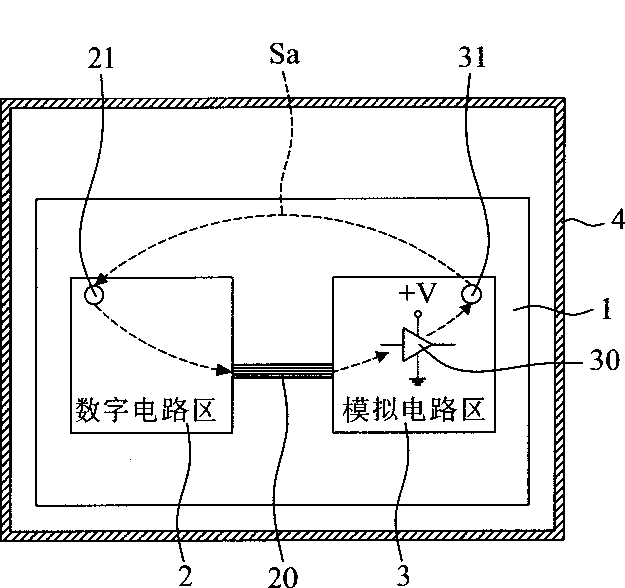
[0015] refer to figure 2 As shown, it is a schematic plan view of an analog circuit ground point of the present invention disposed on the analog circuit area of ​​the motherboard of an electronic device. The electronic device is a computer device (such as a notebook computer), and its circuit substrate or motherboard 1 is provided with a separate digital circuit area 2 and an analog circuit area 3 . similar to figure 1 As shown in the schematic diagram of the circuit configuration, figure 2 The digital circuit area 2 on the motherboard 1 has at least one ground terminal 21, and the ground terminal 21 is connected to the metal casing 4 of the electronic device. Similarly, the analog circuit area 3 also has at least one ground terminal 31 , and the ground terminal 31 is connected to the metal casing 4 of the electronic device. The usual practice is to lock and position the motherboard 1 and the metal casing 4 of the electronic device through known locking screws (not shown)...


PUM


Abstract

This is a structure of eliminating the audio noise and yawp of a electronic device. It's used to avoid the output signals of the sound-source organ in the analog circuit section of the host board of the electronic device from coming back to sound-source organ through the digital circuit section to cause the noise of the audio signals. This invention equips at least one analog loop grounding point at the contiguous position of the signal input end of the sound-source in the analog circuit section. The grounding point of the analog circuit is connected to the metal machine shell of the electronic device, and forms a noise leading loop with the signal input end of the sound-source organ, the output end of the sound-source organ and the grounding point of the analog circuit, to get rid of the audio noise and yawp of the analog section.

Description

technical field [0001] The invention relates to a technology for preventing audio noise and noise, in particular to an audio noise and noise elimination structure of an electronic device, which can be used to prevent audio noise and noise in the analog circuit area on the main board of the electronic device. Background technique [0002] When electronic devices, computer devices, computer peripheral devices or other electronic devices transmit signals, a certain degree of electromagnetic wave interference (radiated emission and conducted emission, referred to as EMI) will be generated in the signal transmission lines, circuit wiring or electronic components themselves. If the electronic product emits excessive EMI noise, it will interfere with the normal operation of electronic components, and even cause the systems or components of other electronic products to fail to work normally. Therefore, the international and various countries have their own standards for EMI testing ...

Claims


Application Information

Patent Timeline
IPC IPC(8): G06F1/00H04B15/00H05K9/00
Inventor 樊用康郑裕强
Owner SHUNDA COMP FACTORY SHUNDE CITY
Why Eureka
Try Eureka