
Image display device and its driving method

A technology of an image display device and a driving method, which can be applied to static indicators, cathode ray tube indicators, instruments, etc., and can solve the problems of increased writing times and increased power consumption.

Inactive Publication Date: 2004-11-24
PANASONIC CORP
View PDF1 Cites 0 Cited by
  • Summary
  • Abstract
  • Description
  • Claims
  • Application Information

AI Technical Summary

Problems solved by technology

However, as the number of writes in subfield groups increases, power consumption due to write operations also increases

Method used


Image

  • Image display device and its driving method
  • Image display device and its driving method
  • Image display device and its driving method

Examples


Embodiment 1

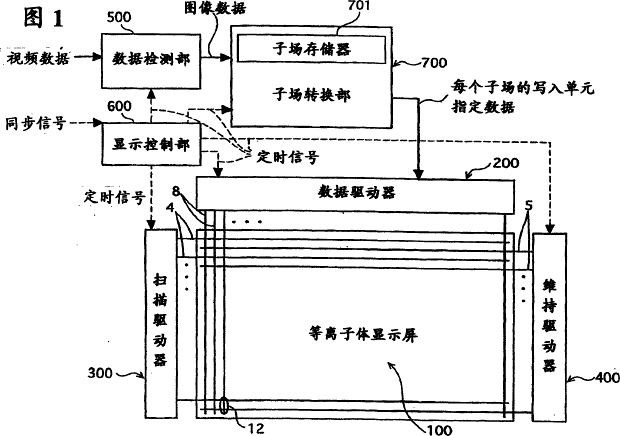
[0036] FIG. 1 is a structural diagram of the PDP device of this embodiment.

[0037] The PDP device shown in FIG. 1 is composed of PDP 100 , data driver 200 , scan driver 300 , sustain driver 400 , data detection unit 500 , display control unit 600 , and subfield conversion unit 700 .

[0038] The PDP 100 is provided with a pair of front plate and back plate. On the front plate side, a plurality of scanning electrodes 4 and a plurality of sustain electrodes 5 extending along the horizontal direction of the screen are arranged, and on the back plate side, a plurality of scanning electrodes 4 extending in the vertical direction of the screen are arranged. Data electrode 8.

[0039] The plurality of scan electrodes 4 , the plurality of sustain electrodes 5 and the plurality of data electrodes 8 are all arranged in a matrix.

[0040] Discharge cells 12 are formed at intersections of scan electrodes 4 , sustain electrodes 5 , and data electrodes 8 . Each discharge cell 12 is fill...

Embodiment 2

[0122] In this embodiment, the number L of writing subfields in a given unit is also set according to the number of times in the immediately preceding field.

[0123] Fig. 7 is a partial structural diagram of the PDP device of this embodiment.

[0124] The overall structure of the PDP apparatus of this embodiment is the same as that of Embodiment 1 shown in FIG. Therefore, only the data detection unit 500, the subfield conversion unit 700 and their peripheral parts are shown in FIG. 7 .

[0125] In this embodiment, the point that the data detection unit 500 transfers sequentially input image data to the subfield conversion unit 700 is the same as that of the first embodiment above, but detects a signal indicating the previous field in the same discharge cell as the input image data. Information on the frequency of sustain discharge (lighting) completed in the subfield (hereinafter referred to as “immediate previous lighting information”), and the detected immediate previous l...


PUM


Abstract

The present invention reduces degradation in image quality caused by a write defect. This is achieved in the following manner. When driving an image display device in which a plurality of cells are arranged to display an image in gray level, by, for each of the plurality of cells, performing a writing operation in sub-fields selected from N sub-fields which form one field and each have a luminance weight, based on an input image signal for the cell, if the writing operation and light emission are performed in the cell in any sub-field in a sub-field group which is constituted by M consecutive sub-fields in the N sub-fields, where 2□M□N, the light emission is sustained in the cell throughout all succeeding sub-fields in the sub-field group, and the number of sub-fields in the sub-field group in which the writing operation is to be performed in the cell L is determined based on at least one of the input image signal for the cell for the field and an input image signal for the cell for an immediately previous field, and the writing operation is performed in each of the selected sub-fields.

Description

technical field [0001] The present invention relates to an image display device represented by a plasma display device and a driving method thereof. Background technique [0002] In recent years, plasma display panels (Plasma Display Panels, hereinafter referred to as PDPs) have attracted attention as display devices used in computers, televisions, etc., because they can be large, thin, and lightweight. [0003] There is also a DC type in the PDP, but now the AC type has become the mainstream. [0004] Generally speaking, in the AC-type main surface discharge PDP, a pair of front plates and back plates are disposed opposite to each other, and strip-shaped scan electrode groups and sustain electrode groups are formed parallel to each other on the opposite surfaces of the front plates, and a dielectric layer is covered on them. In addition, a strip-shaped data electrode group is arranged on the opposite surface of the back plate to perpendicularly intersect with the scanning ...

Claims


Application Information

Patent Timeline
Patent Type & Authority Applications(China)
IPC IPC(8): G09G3/20G09G3/292G09G3/293G09G5/10
CPCG09G2320/0266G09G3/2022G09G2320/0238G09G3/2932G09G3/2927G09G2320/0261G09G3/292G09G3/296
Inventor 武田实增田真司
Owner PANASONIC CORP
Learn More