Semiconductor device and mfg. method thereof

A manufacturing method and semiconductor technology, applied in the fields of semiconductor/solid-state device manufacturing, semiconductor devices, semiconductor/solid-state device components, etc., can solve the problems of poor manufacturing efficiency and limited freedom of semiconductor chips, and achieve the effect of preventing leakage current.

Inactive Publication Date: 2004-10-06
SEIKO EPSON CORP
View PDF1 Cites 6 Cited by
  • Summary
  • Abstract
  • Description
  • Claims
  • Application Information

AI Technical Summary

Problems solved by technology

[0009] On the other hand, since many processes are required to form the above-mentioned electrode structure, there is a problem of poor manufacturing efficiency.
In addition, in the above-mentioned electrode structure, it is necessary to form a through-hole, and depending on the position of the through-hole, the degree of freedom in semiconductor chip design may be limited, so an electrode structure that considers the degree of freedom in design is required.

Method used


Image

  • Semiconductor device and mfg. method thereof
  • Semiconductor device and mfg. method thereof
  • Semiconductor device and mfg. method thereof

Examples


Embodiment Construction

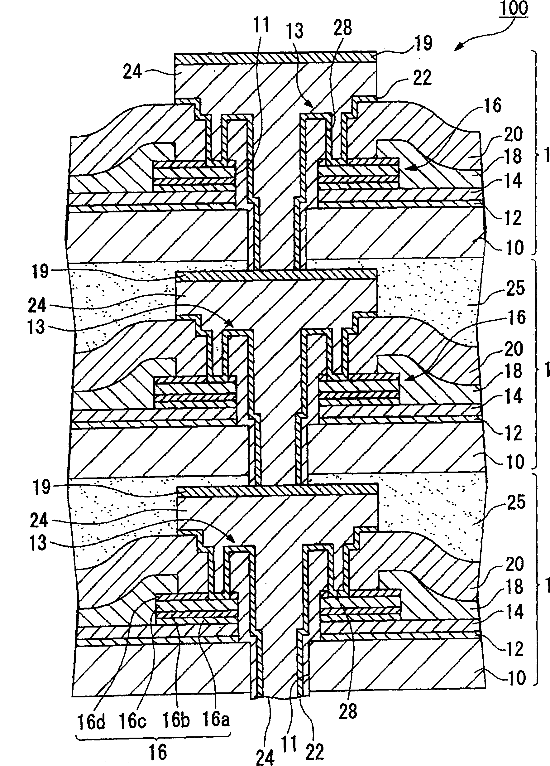
[0041] Embodiments of the present invention will be described below with reference to the drawings. In addition, in the present embodiment, in each figure, different scales are used for each layer and each member so that each layer or each member can be seen clearly on the drawing.

[0042] figure 1 A schematic cross-sectional view showing the main parts of the semiconductor device according to the first embodiment. A semiconductor device 100 is formed by stacking electrode pads on a silicon substrate 10 with an insulating film 12 formed of a thermally oxidized film and an interlayer insulating film 14 formed of SiO2. 16 is formed by three-dimensionally mounting the semiconductor device main body 1 .

[0043] The semiconductor device main body 1 is formed by laminating an insulating film 12 with a thickness of about 4000 Å, an interlayer insulating film 14 with a thickness of about 10000 Å, and an electrode pad 16 with a thickness of about 8000 Å on a silicon substrate 10, an...


PUM


Abstract

A semiconductor device includes a semiconductor device body section having a substrate and an electrode formed on the substrate. A through-hole is formed through the electrode and the substrate in a stacking direction of the electrode and the substrate, and a conductive member is inserted into the through-hole. An insulating material which faces at least the through-hole is formed on the electrode. The conductive member is formed over the insulating material from the through-hole and is connected with the electrode.

Description

technical field [0001] The invention relates to a semiconductor device and its manufacturing method, in particular to a semiconductor device suitable for three-dimensional mounting technology. Background technique [0002] Today, portable electronic devices such as mobile phones, notebook computers, and PDAs (Personal Data Assistance) have achieved miniaturization of various electronic components such as semiconductor chips installed inside in order to be compact and light. , and the space for installing its electronic components is greatly limited. For this reason, for example, in a semiconductor chip, efforts have been made on its packaging method, and a packaging technology called CSP (Chip Scale Package: Chip Scale Package) has been proposed at present. [0003] This kind of semiconductor chip manufactured by using CSP technology can realize high-density mounting because its mounting area is at the same level as that of the semiconductor chip. [0004] However, it can ...

Claims


Application Information

Patent Timeline
Patent Type & Authority Applications(China)
IPC IPC(8): H01L23/52H01L21/3205H01L21/768H01L23/48H01L25/065H01L25/07H01L25/18
CPCH01L21/76898H01L2225/06527H01L2225/06541H01L2924/07811H01L25/50H01L2224/16145H01L2225/06513H01L23/481H01L25/0657H01L2924/00
Inventor 增田员拓
Owner SEIKO EPSON CORP
Why Eureka
Try Eureka