Red light emitted compound used for organic electroluminous device and orgainic electroluminous device using same
A technology of electroluminescent devices and compounds, applied in electroluminescent light sources, organic semiconductor devices, organic chemistry, etc., can solve the problems of low red chroma, incomplete chroma, and reduced quenching luminous efficiency
- Summary
- Abstract
- Description
- Claims
- Application Information
AI Technical Summary
Problems solved by technology
Method used
Image
Examples
Embodiment 1
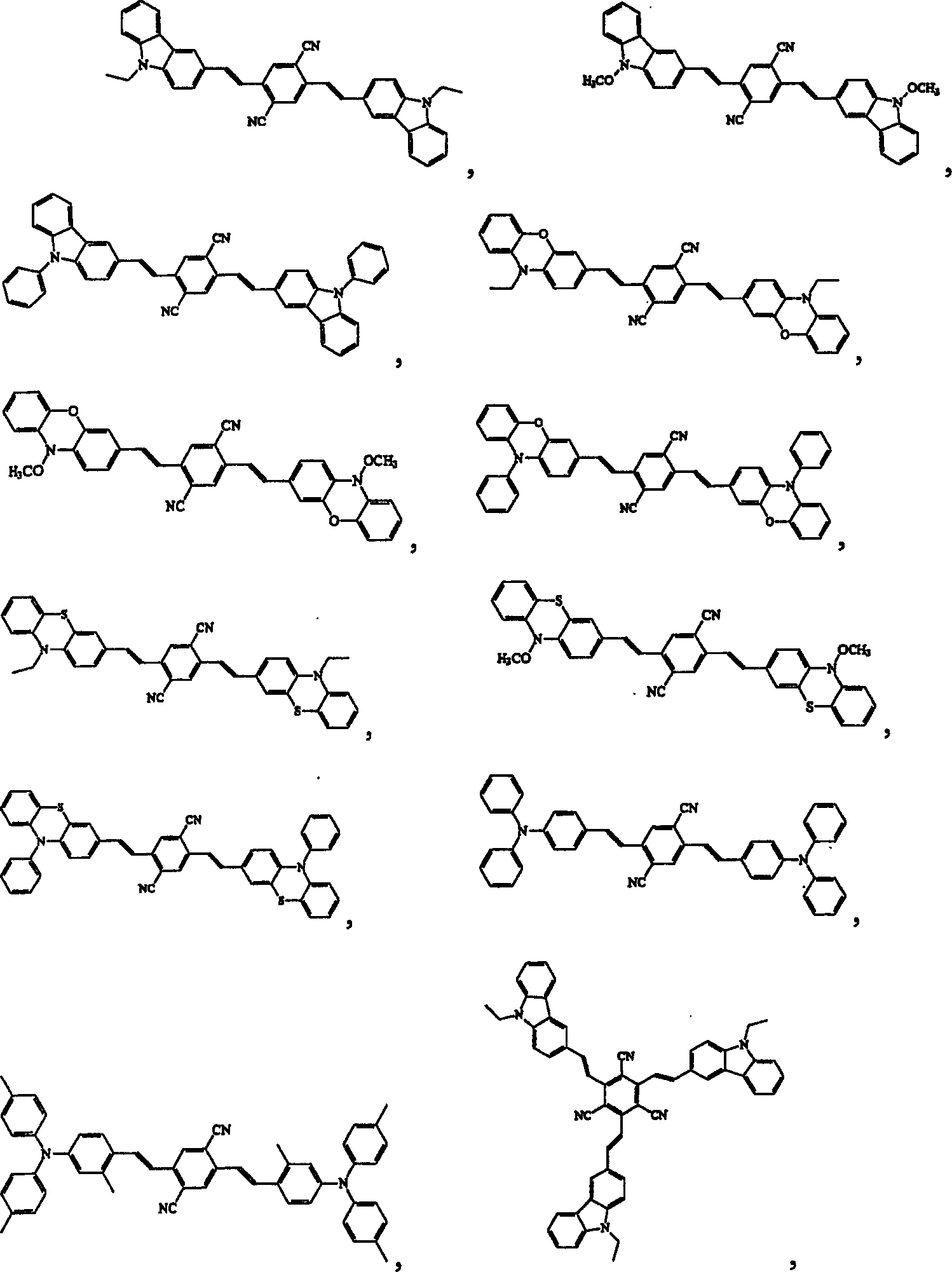
[0129]In this example, an organic EL device using Compound 10 as a dopant and Alq3 as a host for a red-emitting emitting layer was fabricated.
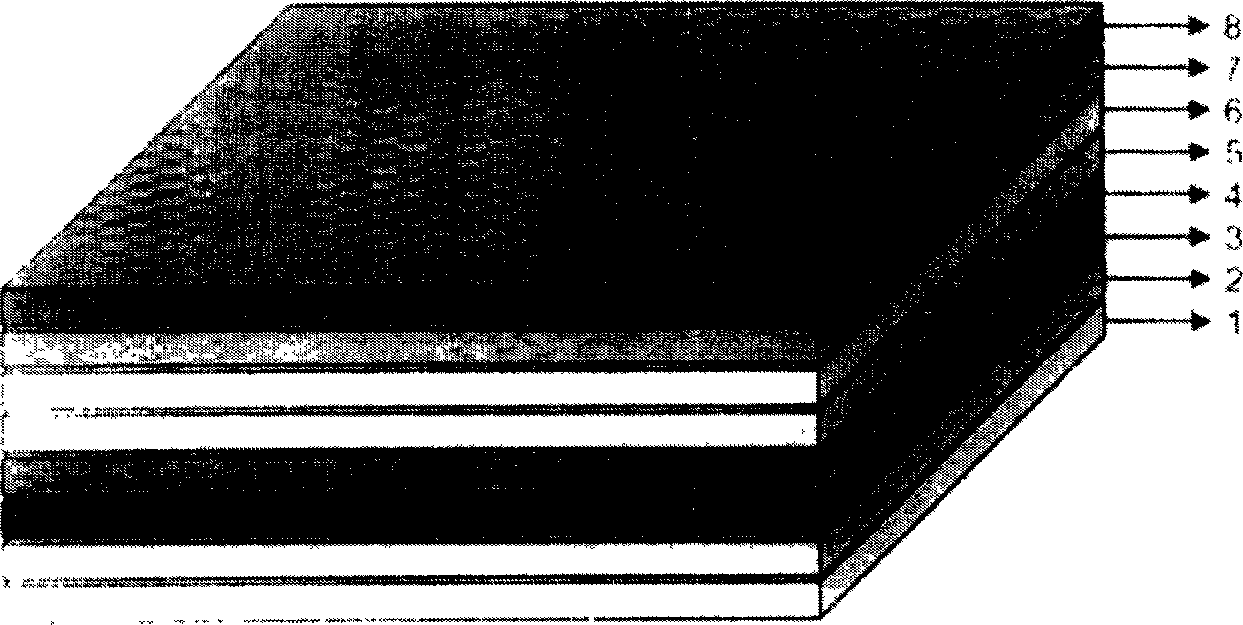
[0130] First, CuPC (copper(II) phthalocyanine) was vacuum-deposited to a thickness of 30 nm on ITO-deposited glass washed with microwaves to form a hole injection layer. Then, NPD (N,N′-dinaphthyl-N,N′-diphenyl-(1,1′-biphenylyl)-4,4′-diamine) was vacuum-deposited thereon to a thickness of 50 nm After the hole transport layer was formed, Alq3 (host) was deposited with a thickness of 30 nm on the hole transport layer to form an emission layer, and Alq3 was doped with 1.0% of compound 10 (dopant). Electron transport layer (Alq3; 40nm), electron injection layer (Li 2 O; 25nm) and a cathode (Mg / Ag; 100nm), thereby obtaining an organic EL device.
[0131] A direct voltage of forward bias was applied to the organic EL device prepared in Example 1, and its luminous performance was evaluated. The glowing color is red. The result of the spe...
Embodiment 2
[0133] In this example, an organic EL device using Compound 1 as a host and DCM as a dopant for a red emitting layer was fabricated.
[0134] First, CuPC with a thickness of 30 nm was vacuum-deposited on ITO-deposited glass washed with microwaves to form a hole-injection layer. Then, NPD (N,N'-dinaphthyl-N,N'-phenyl-(1,1'-biphenyl)-4,4'-diamine) was vacuum-deposited on it to a thickness of 50 nm to form A hole transport layer, and then deposit compound 1 (host) with a thickness of 30 nm on the hole transport layer to form an emission layer, and compound 1 is doped with 1.0% DCM (dopant). Electron transport layer (Alq3; 40nm), electron injection layer (Li 2 O; 25nm) and a cathode (Mg / Ag; 100nm), thereby obtaining an organic EL device.
[0135] A forward bias DC voltage was applied to the organic EL device prepared in Example 2, and its luminous performance was evaluated. The glowing color is red. The result of the spectroscopic test is that the luminescence peak of the spec...
Embodiment 3
[0137] In this example, an organic EL device using Compound 22 as a host and DCM as a dopant for a red emitting layer was fabricated.
[0138] First, CuPC with a thickness of 30 nm was vacuum-deposited on ITO-deposited glass washed with microwaves to form a hole-injection layer. Then, NPD (N,N'-dinaphthyl-N,N'-phenyl-(1,1'-biphenyl)-4,4'-diamine) was vacuum-deposited on it to a thickness of 50 nm to form A hole transport layer, and then deposit compound 22 (host) with a thickness of 30 nm on the hole transport layer to form an emission layer, and compound 22 is doped with 1.0% DCM (dopant). Electron transport layer (Alq3; 40nm), electron injection layer (Li 2 O; 25nm) and a cathode (Mg / Ag; 100nm), thereby obtaining an organic EL device.
[0139] A forward bias DC voltage was applied to the organic EL device prepared in Example 3, and its luminous performance was evaluated. The glowing color is red. The result of the spectroscopic test is that the luminescence peak of the s...
PUM
| Property | Measurement | Unit |
|---|---|---|
| thickness | aaaaa | aaaaa |
| thickness | aaaaa | aaaaa |
| melting point | aaaaa | aaaaa |
Abstract
Description
Claims
Application Information
 - R&D
- Intellectual Property
- Life Sciences
- Materials
- Tech Scout
- Unparalleled Data Quality
- Higher Quality Content
- 60% Fewer Hallucinations
Browse by: Latest US Patents, China's latest patents, Technical Efficacy Thesaurus, Application Domain, Technology Topic, Popular Technical Reports.
© 2025 PatSnap. All rights reserved.Legal|Privacy policy|Modern Slavery Act Transparency Statement|Sitemap|About US| Contact US: help@patsnap.com


