


Quick Research
Generate reliable direction feasibility study reports for your R&D in just a few steps.

Technical Q&A
Discover and master advanced knowledge NOW. Basics, ideas, possibilities, all at once.

Find Solutions
As an expert in R&D theories, this can generate solutions to your technical problems instantly.

Evaluate Feasibility
Analyze your overall solution with one click, know your potential R&D risks in advance.

Monitor Landscape
Get weekly tech updates, stay abreast of the latest tech innovations and key insights.
Producing device for electro-optical device, electro-optic device, and electronic instruments
An electro-optical device and manufacturing device technology, applied in instruments, respiratory filters, optics, etc., can solve problems such as impurities mixed in, liquid crystal display quality degradation, etc.
- Summary
- Abstract
- Description
- Claims
- Application Information
AI Technical Summary
Problems solved by technology
Method used
Image

Examples
Embodiment 1
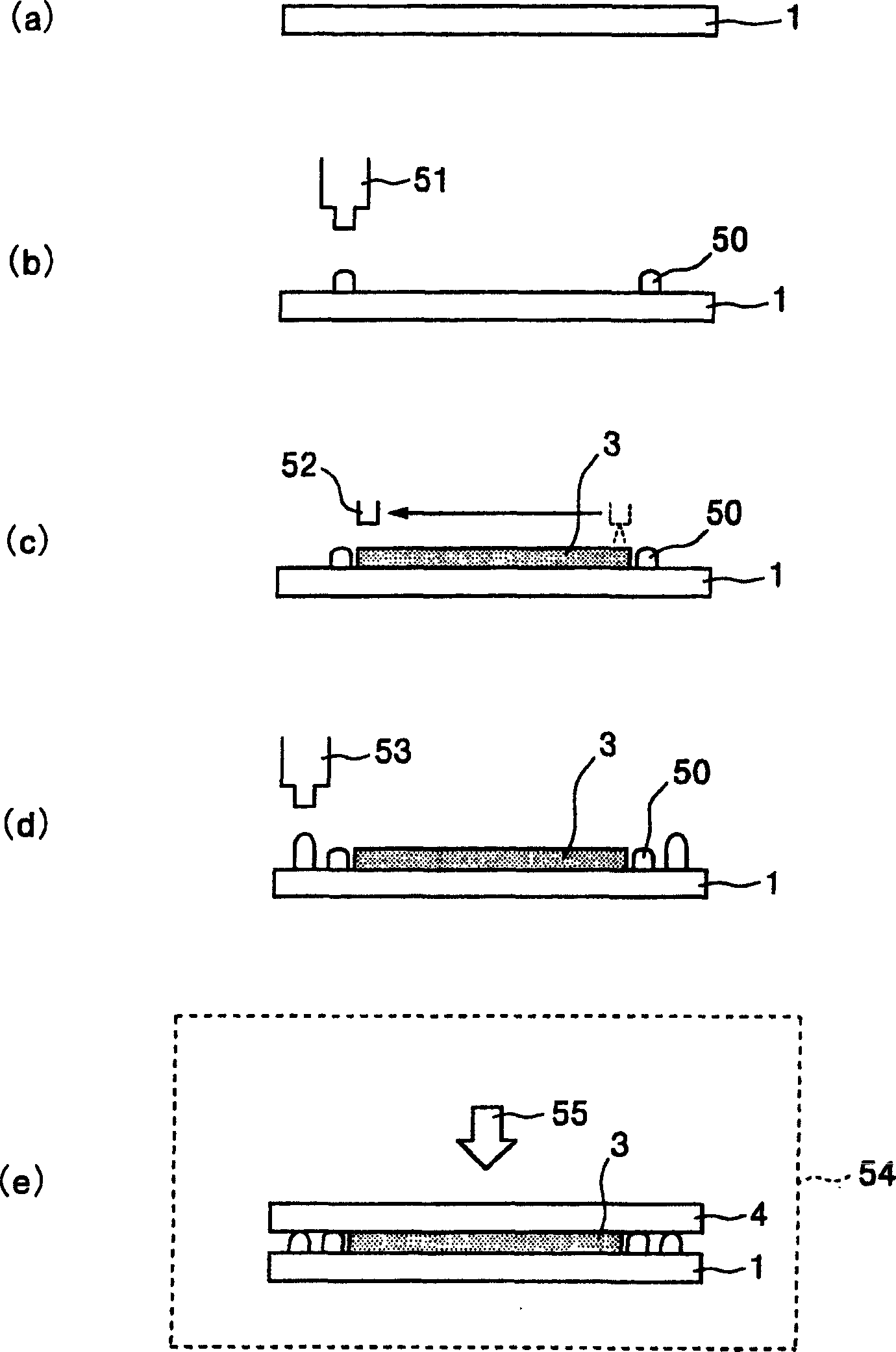
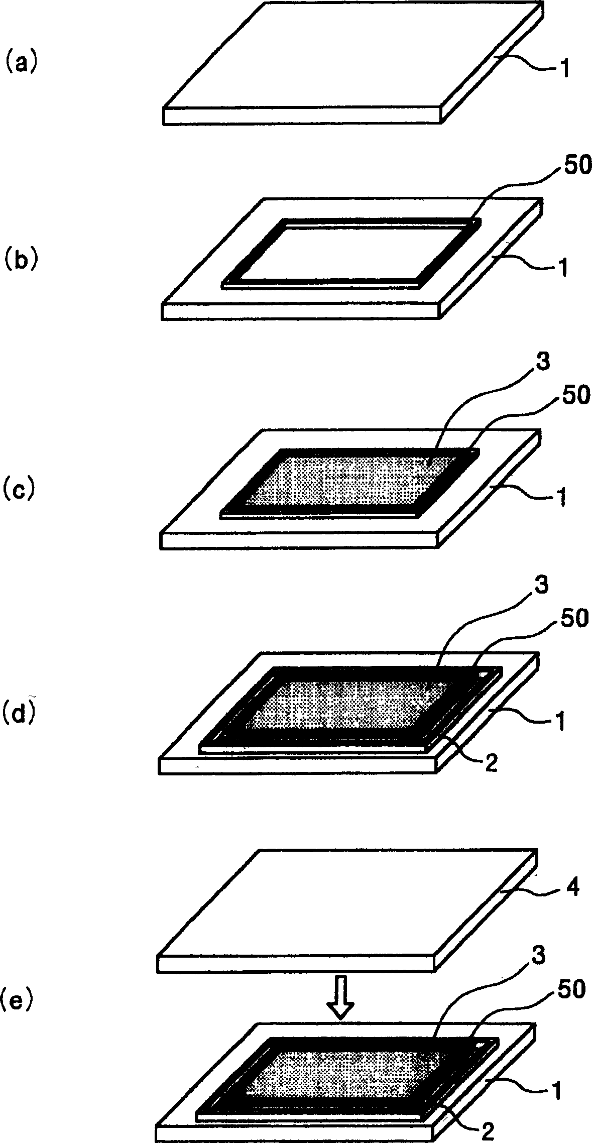
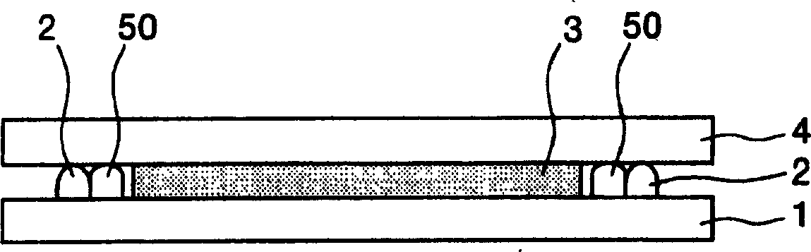
[0043] First, refer to Figure 4 The structure of the liquid crystal display panel which is the electro-optic device of the present invention will be described. The liquid crystal display panel 100 of this embodiment has a first substrate 1 and a second substrate 4 arranged oppositely, and liquid crystal display elements 106 and 107 are respectively formed on the inner surfaces of the first substrate 1 and the second substrate 4 .
[0044] Specifically, as Figure 4 As shown, a reflective film (aluminum, silver) 101, a color filter (CF) 102, a protective (OVC) layer 103, a transparent electrode 104, and an alignment film 105 are sequentially formed on the first substrate 1 as the first substrate side. Liquid crystal display element 106.
[0045] On the other hand, a transparent electrode 104 and an alignment film 105 are formed on the opposite second substrate 4 . The transparent electrode 104 is formed of a transparent electrode material such as ITO (Indium Tin Oxide), pro...
Embodiment 2
[0079] Below, refer to Figure 8 with Figure 9 Specific examples of electronic equipment to which the liquid crystal display panel of the present invention can be applied will be described.
[0080] First, an example in which the liquid crystal display panel of the present invention is applied to a display portion of a portable personal computer (so-called notebook computer) will be described. Figure 8 It is a perspective view showing the mechanism of this personal computer. Such as Figure 8 As shown, a personal computer 91 has a main body 912 provided with a keyboard 911, and a display 913 to which a liquid crystal display panel of the present invention is applied.
[0081] Next, an example in which the liquid crystal display panel of the present invention is applied to a display portion of a mobile phone will be described.
[0082] Such as Figure 9 As shown, in addition to a plurality of operation buttons 921, a mobile phone 92 also has a receiver port 922, a speake...
PUM
 Abstract
Description
Claims
Application Information
 - R&D Engineer
- R&D Manager
- IP Professional
- Industry Leading Data Capabilities
- Powerful AI technology
- Patent DNA Extraction
Browse by: Latest US Patents, China's latest patents, Technical Efficacy Thesaurus, Application Domain, Technology Topic, Popular Technical Reports.
© 2024 PatSnap. All rights reserved.Legal|Privacy policy|Modern Slavery Act Transparency Statement|Sitemap|About US| Contact US: help@patsnap.com