Electrooptical device and electronic appliance

An electro-optical device and electrode technology, which can be used in identification devices, optics, circuits, etc., can solve the problems of inability to achieve aperture ratio and increase, and achieve the effects of miniaturization, reduction in potential variation, and high contrast.

Inactive Publication Date: 2004-05-26
138 EAST LCD ADVANCEMENTS LTD
View PDF0 Cites 11 Cited by
  • Summary
  • Abstract
  • Description
  • Claims
  • Application Information

AI Technical Summary

Problems solved by technology

[0008] As mentioned above, the improvement of the aperture ratio cannot be achieved by merely increasing the area of ​​the light-transmitting region, and comprehensive measures must be taken from all aspects in order to achieve this goal.

Method used


Image

  • Electrooptical device and electronic appliance
  • Electrooptical device and electronic appliance
  • Electrooptical device and electronic appliance

Examples


Embodiment Construction

[0147] Embodiments of the present invention will be described below with reference to the accompanying drawings. In the following embodiments, the electro-optical device of the present invention is used in a liquid crystal device.

[0148] 1st form of implementation

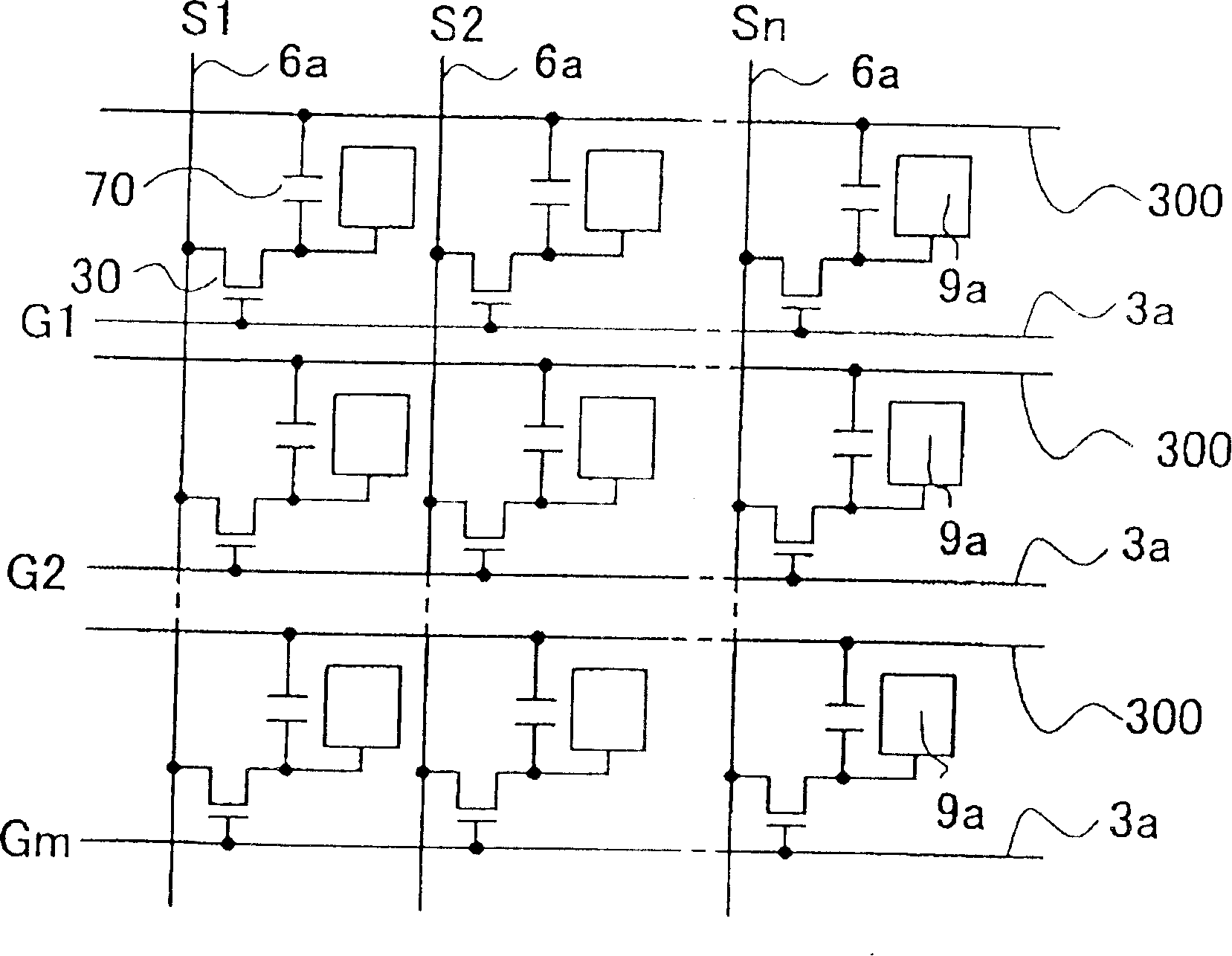
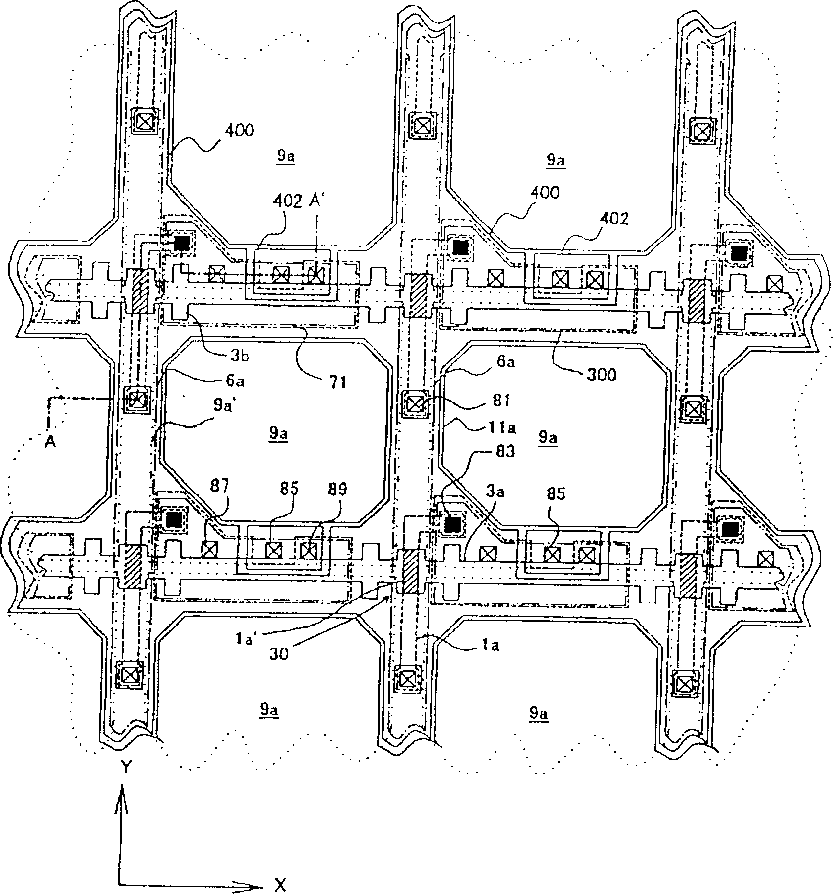
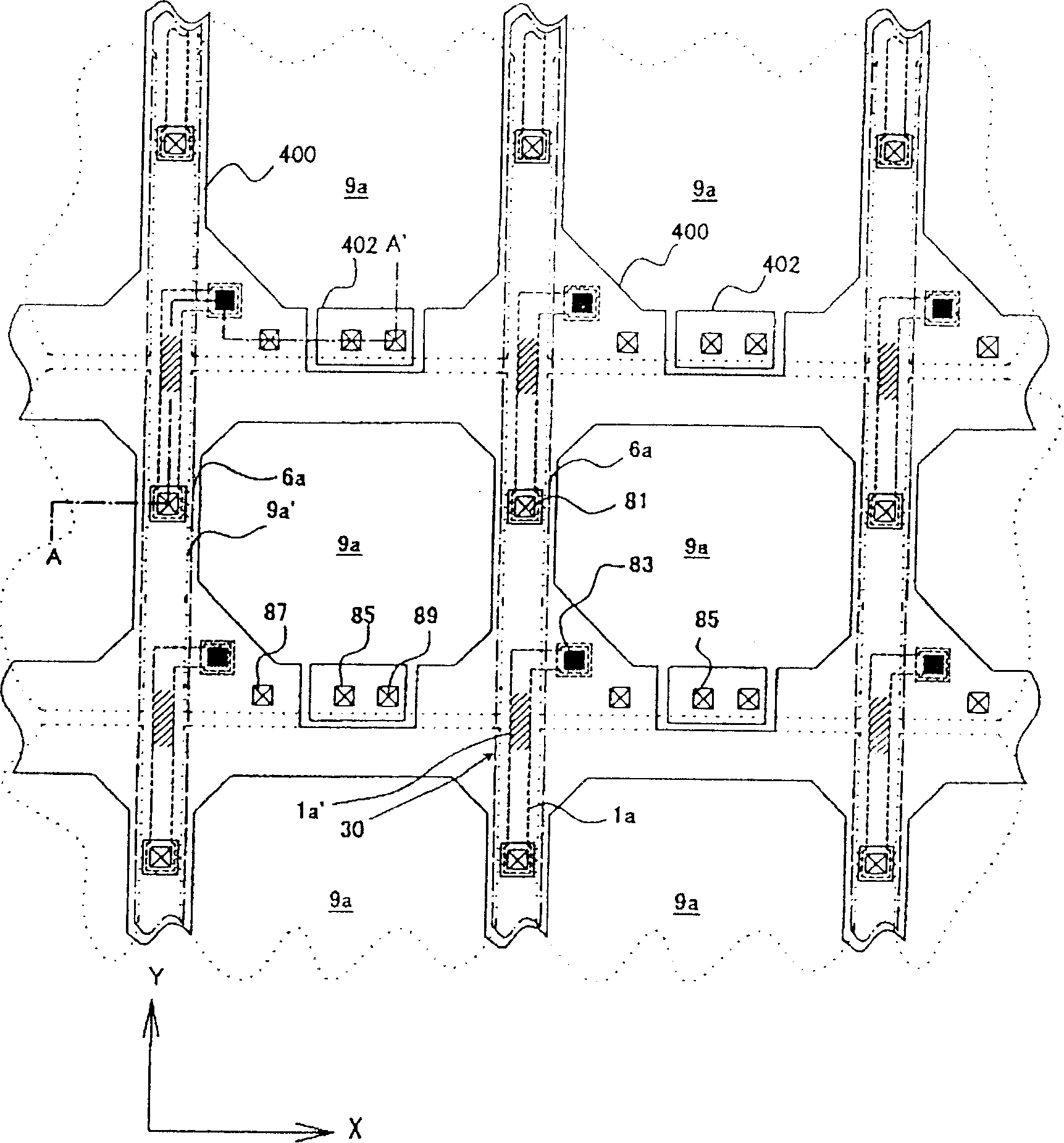
[0149] First, refer to Figure 1 to Figure 4 , the configuration of the pixel portion of the electro-optical device according to the first embodiment of the present invention will be described. here, figure 1 It is an equivalent circuit of various elements, wiring, and the like in a plurality of pixels formed in a matrix forming an image display region of an electro-optical device. figure 2 It is a plan view of a plurality of adjacent pixel groups of a TFT array substrate on which data lines, scanning lines, pixel electrodes, etc. are formed. in addition, image 3 will be figure 2 The main part in , specifically, is a plan view in which only data lines, shield layers, and pixel electrodes are selected in ...


PUM

PropertyMeasurementUnit
thicknessaaaaaaaaaa

Abstract

An electro-optical device includes: data lines extending in a first direction above a substrate; scanning lines extending in a second direction and intersecting the data lines; pixel electrodes and thin-film transistors arrayed so as to correspond to intersection regions of the data lines and the scanning lines; capacitors formed at a layer higher than the semiconductor layer of the thin-film transistors and at a layer lower than the pixel electrodes, and electrically connected to pixel potential; and upper light shielding film positioned between the data lines and the pixel electrodes; the upper light shielding film defining at least the corners of pixel opening regions; and the scanning lines, the data lines, and the capacitors, being formed in the light shielded region.

Description

technical field [0001] The present invention relates to the technical field of electro-optical devices such as liquid crystal devices and electronic equipment. In addition, the present invention also relates to technical fields such as electrophoretic devices such as electronic paper, EL (Electroluminescence) devices, and devices using electron emission elements (Field Emission Display and Surface-Conduction Electron-Emitter Display). Background technique [0002] Conventionally, electro-optical devices such as liquid crystal devices are known in which an electro-optic material such as liquid crystal is interposed between a pair of substrates, and light is transmitted through the substrates so as to display images. The "display of an image" here is realized by, for example, changing the state of the electro-optic material for each pixel to change the transmittance of light so that light with different gradations can be recognized for each pixel. [0003] As such an electro-...

Claims


Application Information

Patent Timeline
Patent Type & Authority Applications(China)
IPC IPC(8): G02F1/1368G02F1/1335G02F1/1362G02F1/167G09F9/30H01L51/50
CPCG02F1/167G02F1/136213G02F1/136209G02F1/1335
Inventor 恒川吉文仓科久树清水雄一
Owner 138 EAST LCD ADVANCEMENTS LTD
Why Eureka
Try Eureka