Capacitance element and mfg method thereof
A technology of capacitive elements and manufacturing methods, which is applied in the direction of electrical components, fixed capacitance parts, capacitors, etc., can solve problems such as complex electrode structures, and achieve the effects of reducing deviation, reducing characteristic deviation, and reducing characteristic deviation
- Summary
- Abstract
- Description
- Claims
- Application Information
AI Technical Summary
Problems solved by technology
Method used
Image

Examples
no. 1 Embodiment approach
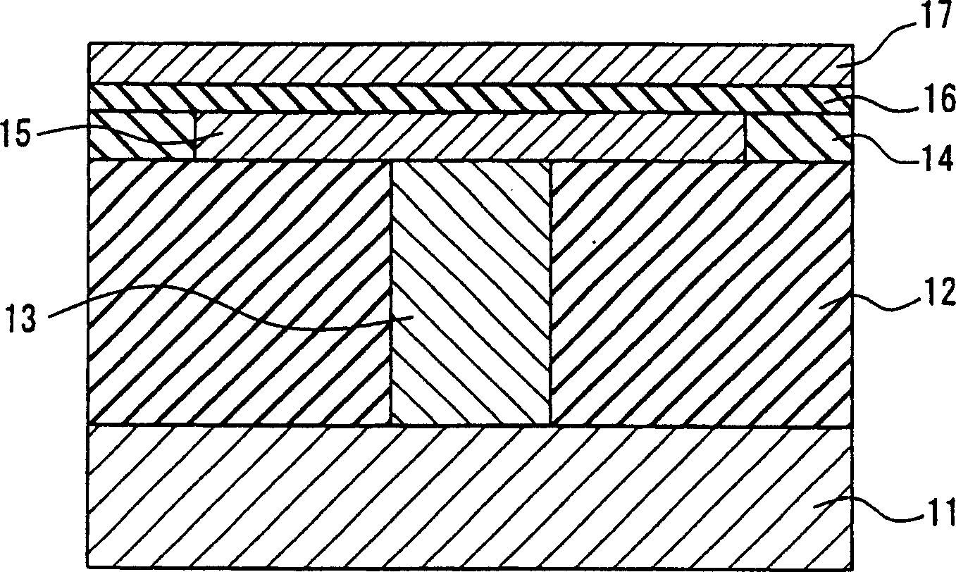
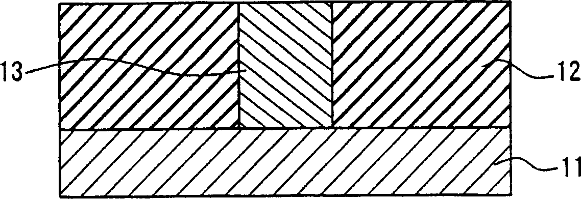
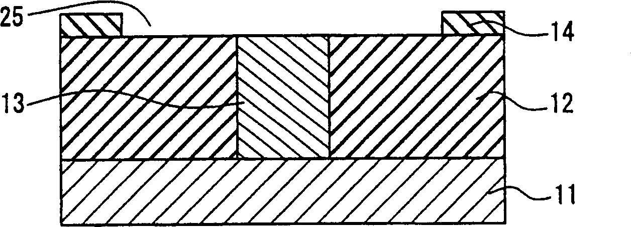
[0033] Hereinafter, a first embodiment of the present invention will be described in detail with reference to the drawings. figure 1 11 is a Si substrate, 12 is an insulating film such as a silicon oxide film, 13 is a contact plug made of polysilicon (PS) or tungsten (W), and 14 is an oxide film. An insulating film such as a silicon film, 15 is a lower electrode made of Pt, and 16 is made of SBT (SrBi 2 Ta 2 o 9 ) composed of a ferroelectric thin film, 17 is an upper electrode composed of Pt. The film thickness of the lower electrode 15 is 50 nm, and the film thickness variation is controlled within 10%. By controlling the film thickness of the lower electrode in this way, when the ferroelectric thin film 16 is produced by the MOCVD method, it is possible to prevent the Bi metal constituting the ferroelectric thin film 16 from the Pt lower electrode 15 in the capacitive element and between the capacitive elements. Since the amount of diffusion is controlled, it is possibl...
no. 2 Embodiment approach
[0039] Hereinafter, a second embodiment of the present invention will be described in detail with reference to the drawings.
[0040] image 3 is a cross-sectional view showing the capacitive element of the present invention, in image 3 Among them, 31 is a Si substrate, 32 is an insulating film such as a silicon oxide film, 33 is a contact plug made of polysilicon (PS) or tungsten (W), 34 is an insulating film such as a silicon oxide film, and 35 is made of Pt. The lower electrode, 36 is a ferroelectric thin film made of SBT, 37 is an upper electrode made of Pt, and 38 is a concave portion with a depth of 300 nm.
[0041] image 3 The manufacturing method of the capacitive element shown is substantially the same as the method described above in FIG. 2 of the first embodiment except for a part of the process. The difference is that the concave portion 38 is formed deeper, and the lower electrode 35 does not completely fill the concave portion 38, but along the bottom portio...
no. 3 Embodiment approach
[0046] Hereinafter, a third embodiment of the present invention will be described in detail with reference to the drawings.
[0047] Figure 5 A sectional view showing a capacitive element of the present invention, in Figure 5 Among them, 41 is a Si substrate, 42 is an insulating film such as a silicon oxide film, 43 is a contact plug made of polysilicon (PS) or tungsten (W), 43a is an upper extension of the contact plug 43, and 44 is a silicon oxide film. An insulating film such as an oxide film, 45 is a lower electrode made of Pt, 46 is a ferroelectric thin film made of SBT, and 47 is an upper electrode made of Pt.
[0048] exist Figure 5 Among them, the width of the lower electrode 45 is controlled at 40 nm, and the deviation of the width is controlled within 10%. In this way, the lower electrode is not like figure 1 expand horizontally like that, but instead like Figure 5 When extending in the vertical direction in this way, the above-mentioned width of the lower ...
PUM
| Property | Measurement | Unit |
|---|---|---|
| thickness | aaaaa | aaaaa |
| depth | aaaaa | aaaaa |
| thickness | aaaaa | aaaaa |
Abstract
Description
Claims
Application Information
 - R&D
- Intellectual Property
- Life Sciences
- Materials
- Tech Scout
- Unparalleled Data Quality
- Higher Quality Content
- 60% Fewer Hallucinations
Browse by: Latest US Patents, China's latest patents, Technical Efficacy Thesaurus, Application Domain, Technology Topic, Popular Technical Reports.
© 2025 PatSnap. All rights reserved.Legal|Privacy policy|Modern Slavery Act Transparency Statement|Sitemap|About US| Contact US: help@patsnap.com