Organic electroluminescent element

An electroluminescence device and a luminescence technology, which are applied in the direction of electroluminescence light sources, organic semiconductor devices, and electric solid-state devices, can solve problems such as reduced efficiency

Inactive Publication Date: 2004-03-10
SONY CORP
View PDF0 Cites 5 Cited by
  • Summary
  • Abstract
  • Description
  • Claims
  • Application Information

AI Technical Summary

Problems solved by technology

As a result, the efficiency of extracting light from the organic light emitting layer 13b decreases

Method used


Image

  • Organic electroluminescent element
  • Organic electroluminescent element
  • Organic electroluminescent element

Examples


Embodiment Construction

[0017] Hereinafter, an organic EL device according to the present invention will be described based on the drawings.

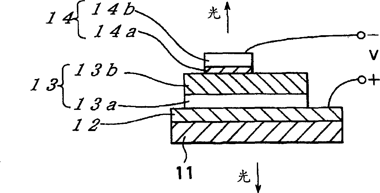
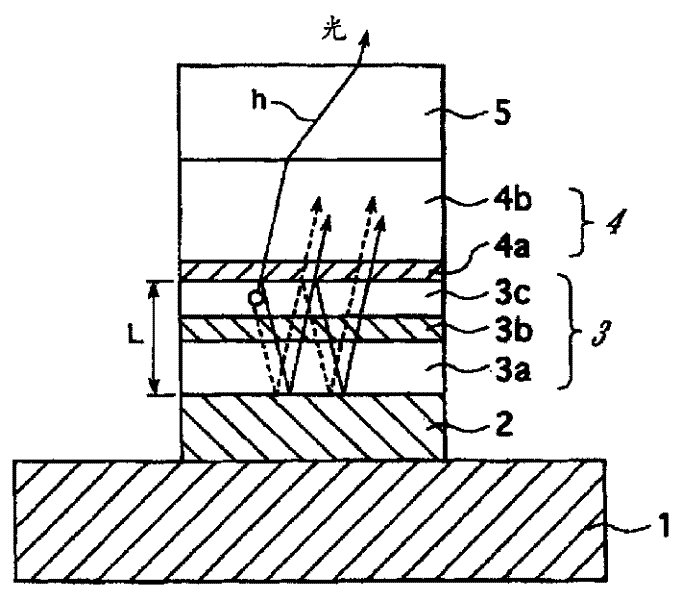
[0018] Now, the case where the present invention is applied to a top emission type organic EL device will be described as an example. The organic EL device described here generally has the same film configuration as the conventional case described above. That is, if figure 1 As shown, the organic EL device has a configuration in which a first electrode 2, an organic layer 3, a second electrode 4, and a passivation film 5 are sequentially stacked on a substrate 1 in this order from bottom to top.

[0019] The substrate 1 is formed of a transparent glass substrate or a semiconductor substrate.

[0020] The first electrode 2 serves as an anode that also serves as a reflective layer, and is formed of a light reflective material such as platinum (Pt), gold (Au), chrome (Cr), tungsten (W), or the like. The film thickness of the first electrode 2 is preferably set...


PUM


Abstract

A self-light-emitting type organic electroluminescence device which makes it possible to restrain to the utmost the absorption of light in an electrode layer, to efficiently take out the light and thereby to obtain sufficient luminance efficiency and the like, in the case of emitting the light through the electrode layer. In an organic electroluminescence device comprising a light-emitting layer ( 3 ) comprised of an organic material based the light-emitting layer ( 3 ) being sandwiched between a first electrode ( 2 ) and a second electrode ( 4 ), and light emitted from the light-emitting layer ( 3 ) being taken out to at least one of the side of the first electrode ( 2 ) and the side of the second electrode ( 4 ), the light absorbance of the electrode or electrodes on the side of taking out the light, of the first electrode ( 2 ) and the second electrode ( 4 ), is not more than 10%.

Description

technical field [0001] The present invention relates to an organic electroluminescent device (hereinafter referred to as "organic EL device"), which is a self-luminous display device. Background technique [0002] In recent years, organic EL devices have attracted attention as display devices constituting flat panel displays. An organic EL device generally has a structure in which an organic material is sandwiched between electrodes (anode and cathode). With the driving current applied to the two electrodes, positive holes and electrons are respectively injected from the two electrodes into the organic layer made of organic materials, and the positive holes and electrons recombine with each other in the organic layer, thereby causing light emission . [0003] As an example of such an organic EL device, there is known a top emission type using a so-called TAC (Top Emission Adaptive Current Drive) technology, such as figure 1 example shown. In the organic EL device shown, ...

Claims


Application Information

Patent Timeline
IPC IPC(8): H05B33/26H01L51/50H01L51/52H05B33/24H05B33/28
CPCH01L2251/5315H01L2251/5323H01L51/5265H01L51/5234H10K50/828H10K50/852H10K2102/3031H10K2102/3026H05B33/24
Inventor 山田二郎
Owner SONY CORP
Why Eureka
Try Eureka