Printed circuitboard
A technology for printed circuit boards and insulating boards, applied in the directions of printed circuits, printed circuit manufacturing, printed circuit components, etc., can solve the problems of high frequency characteristics reduction, signal attenuation, radiation noise reduction, etc., so as to avoid aging and radiation noise. The effect of suppressing and suppressing radiated noise
- Summary
- Abstract
- Description
- Claims
- Application Information
AI Technical Summary
Problems solved by technology
Method used
Image

Examples
no. 1 example
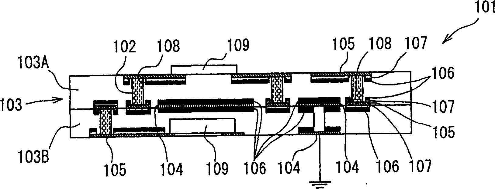
[0059] FIG. 1 is a cross-sectional view of an electronic component built in a printed circuit board 101 according to a first embodiment of the present invention. The printed circuit board 101 has an insulating board 103 . The insulating plate 103 has two layers of electrical insulating layers 103A and 103B, which are integrally formed. Electrically insulating layers 103A and 103B comprise a composite material in which epoxy resin and organic filler are mixed together, such as fused silica or alumina. The electrical insulating layers 103A and 103B have inner through holes 102, and the inner through holes 102 contain thermosetting epoxy resin or the like with conductive particles. The inner through hole 102 passes through the thickness direction of the electrical insulating layers 103A and 103B. The electrical insulating layers 103A and 103B have a signal transmission lead 105 and an auxiliary lead 104. The signal transmission lead 105 and the auxiliary lead 104 are provided on...
no. 2 example
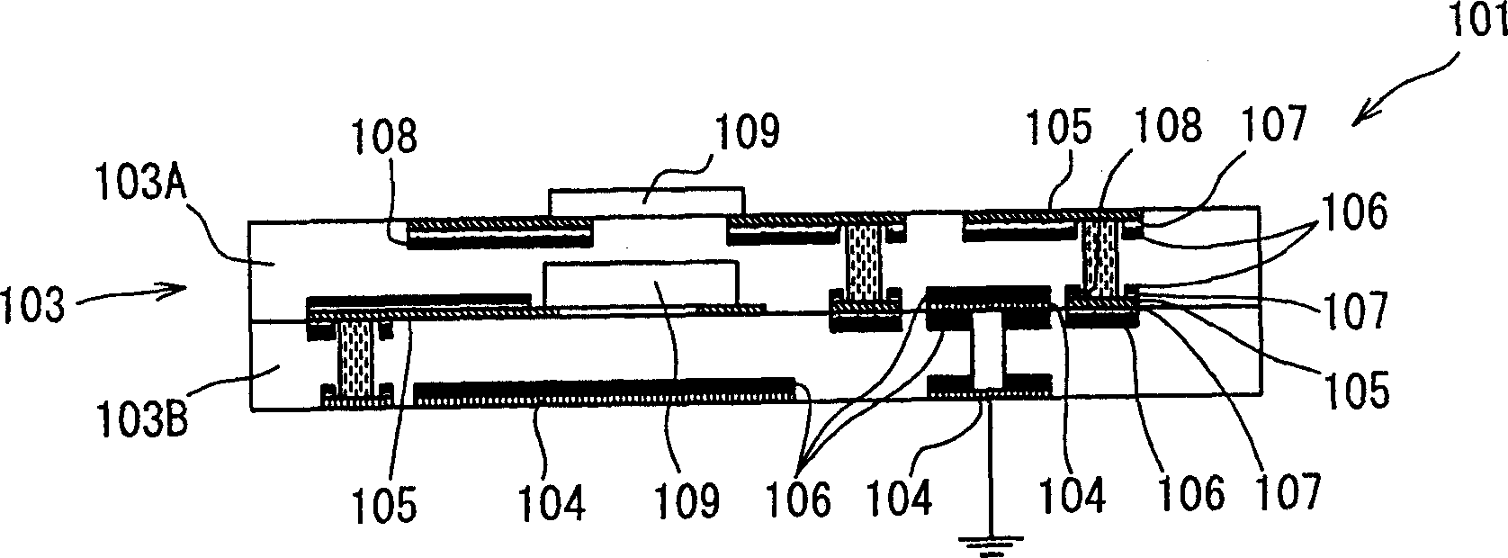
[0072] figure 2 is a cross-sectional view of a printed circuit board electronic component built-in type of the second embodiment. figure 2 The printed circuit board 201 has an insulating board 203 . The insulating plate 203 has double layers of electrical insulating layers 203A and 203B, which are integrally laminated. Electrically insulating layers 203A and 203B comprise a composite material in which epoxy resin and inorganic filler are mixed together, such as fused silica or alumina. The signal transmission lead 205, the auxiliary leads 204A and 204B, and the electronic component 209 are arranged between the layers of the electrical insulating layers 203A and 203B. Auxiliary leads 204A and 204B are arranged between the signal transmission leads 205, the auxiliary lead 204A is connected to the ground potential, on the other hand, the auxiliary lead 204B is not connected to the ground potential (not shown) it becomes so-called non-connection. An electromagnetic shielding ...
no. 4 example
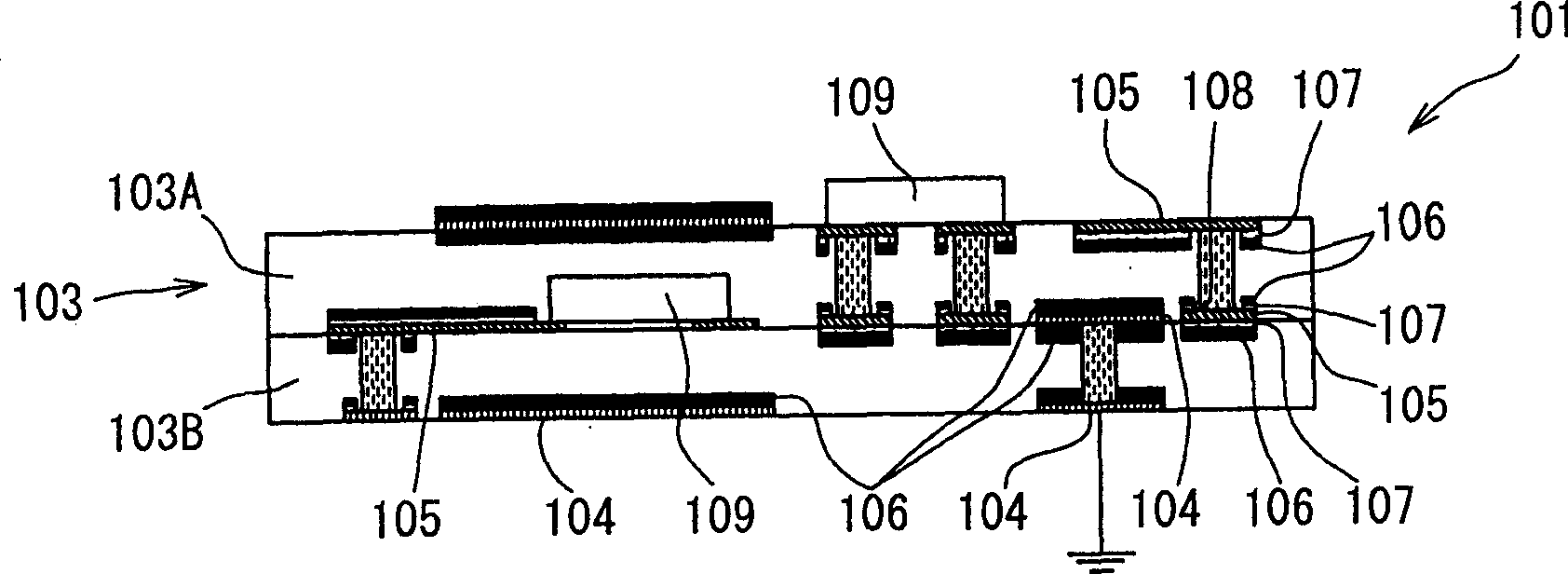
[0082] Fig. 4 is a cross-sectional view of a printed circuit board electronic component built-in type according to a fourth embodiment of the present invention. Figure 4A is a cross-sectional view of a type with built-in printed circuit board electronic components, Figure 4B yes Figure 4A A cross-sectional view along line a-a', Figure 4C is Figure 4A A cross-sectional view along line b-b', Fig. 4D is Figure 4A Sectional view along line c-c', Figure 4E It is an enlarged view of the main part, showing the arrangement of the inner core passing through the hole.
[0083] The electronic component built-in type printed circuit board 401 has an insulating board 403 having four electrical insulating layers 403A to 403D which are integrally laminated. Electronic components 409 are embedded in the interlayer between electrically insulating layers 403 and 403 . The signal transmission lead 405 , the first auxiliary lead 404A, and the second auxiliary leads 404B and 404C are ar...
PUM
 Abstract
Description
Claims
Application Information
 - R&D
- Intellectual Property
- Life Sciences
- Materials
- Tech Scout
- Unparalleled Data Quality
- Higher Quality Content
- 60% Fewer Hallucinations
Browse by: Latest US Patents, China's latest patents, Technical Efficacy Thesaurus, Application Domain, Technology Topic, Popular Technical Reports.
© 2025 PatSnap. All rights reserved.Legal|Privacy policy|Modern Slavery Act Transparency Statement|Sitemap|About US| Contact US: help@patsnap.com