Power control circuit of optical information recording device
A power control and circuit technology, applied in optical recording heads, optical recording/reproducing, circuits, etc., can solve the problems of inability to sample signal level at speed, inability to correct optical signal compensation operation, and high cost.
- Summary
- Abstract
- Description
- Claims
- Application Information
AI Technical Summary
Problems solved by technology
Method used
Image
Examples
no. 1 example
[0044] Please refer to Figure 5 , Figure 5 A block diagram of a power control circuit of a recordable optical disc player according to the first embodiment of the present invention is shown. The laser diode D1 receives the driving signal output from the laser diode driving circuit 502 to generate a corresponding optical signal. The optical signal is irradiated onto an optical disc (not shown in the figure) for burning. In order to perform the optical signal compensation operation, a photodiode (photodiode) D2 senses the optical signal generated by the laser diode D1 and generates a corresponding power sampling signal PI. The power sample signal PI is respectively input to a sample and hold circuit 504 , a peak envelope acquisition circuit 510 , and a bottom envelope acquisition circuit 512 for erasing periods.
[0045] Wherein, the peak envelope acquisition circuit 510 detects the envelope formed by the positive peak of the power sampling signal PI to output the peak enve...
no. 2 example
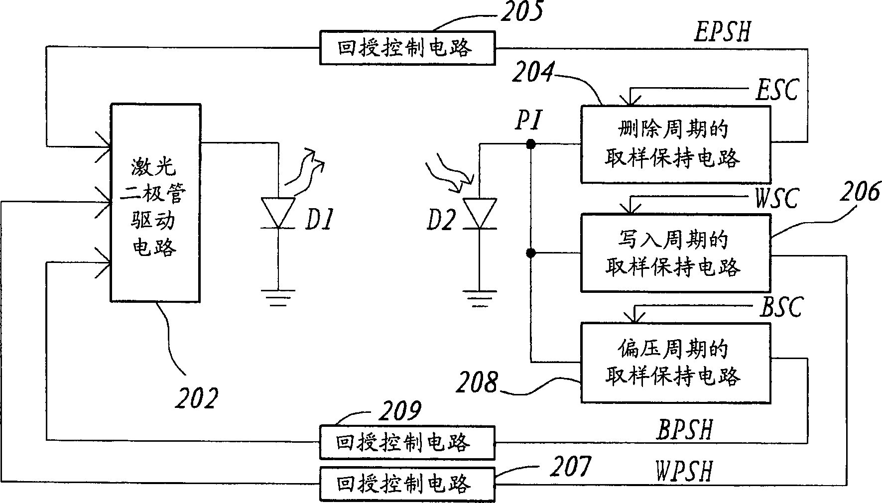
[0053] Please refer to Figure 9 , Figure 9 A block diagram of a power control circuit of a recordable optical disc player according to the second embodiment of the present invention is shown. The laser diode D3 receives the driving signal output from the laser diode driving circuit 902 to generate a corresponding optical signal. The photodiode D4 senses the light signal generated by the laser diode D3 and generates a corresponding power sampling signal PI. The power sampling signal PI is respectively input to the sample-and-hold circuit 904 , the peak envelope sample-and-hold circuit 906 , and the bottom envelope sample-and-hold circuit 908 for erasing periods.
[0054] The sample-and-hold circuit 904 of the erasure period is controlled by an erasure sampling control signal ESC to sample the power sampling signal PI in the erasure period, and output a sample-hold signal EPSH of the erasure period to the feedback control circuit 905 . The feedback control circuit 905 conve...
PUM
 Abstract
Description
Claims
Application Information
 - R&D
- Intellectual Property
- Life Sciences
- Materials
- Tech Scout
- Unparalleled Data Quality
- Higher Quality Content
- 60% Fewer Hallucinations
Browse by: Latest US Patents, China's latest patents, Technical Efficacy Thesaurus, Application Domain, Technology Topic, Popular Technical Reports.
© 2025 PatSnap. All rights reserved.Legal|Privacy policy|Modern Slavery Act Transparency Statement|Sitemap|About US| Contact US: help@patsnap.com


