Exposure device, exposure method and element making method

A technology of exposure device and manufacturing method, which is applied in the direction of photolithographic process exposure device, semiconductor/solid-state device manufacturing, electrical components, etc., can solve the problems of pattern segmentation position limitation, size limitation, difficulty, etc., and achieve the goal of improving bonding accuracy and exposure uniformity effect

Inactive Publication Date: 2007-03-07
NIKON CORP
View PDF4 Cites 0 Cited by
  • Summary
  • Abstract
  • Description
  • Claims
  • Application Information

AI Technical Summary

Problems solved by technology

Moreover, the joint of the divided pattern is only formed at the end of the trapezoidal projected area, so the divided position of the pattern is also limited by it.
As described above, in the known method, the division position of the pattern or the size of the pattern formed on the photosensitive substrate P is limited, and it is difficult to manufacture an arbitrary module.

Method used


Image

  • Exposure device, exposure method and element making method
  • Exposure device, exposure method and element making method
  • Exposure device, exposure method and element making method

Examples


Embodiment Construction

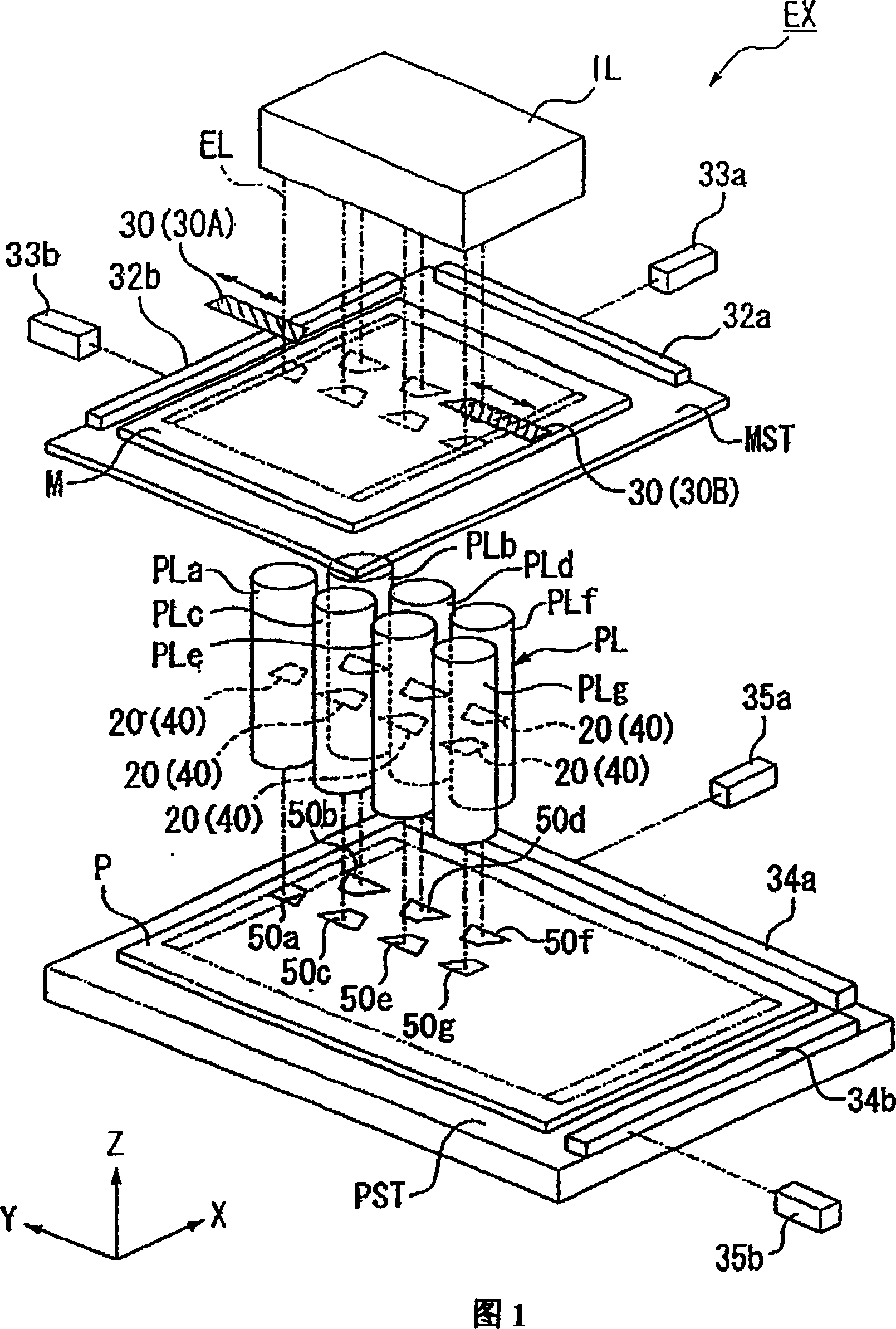
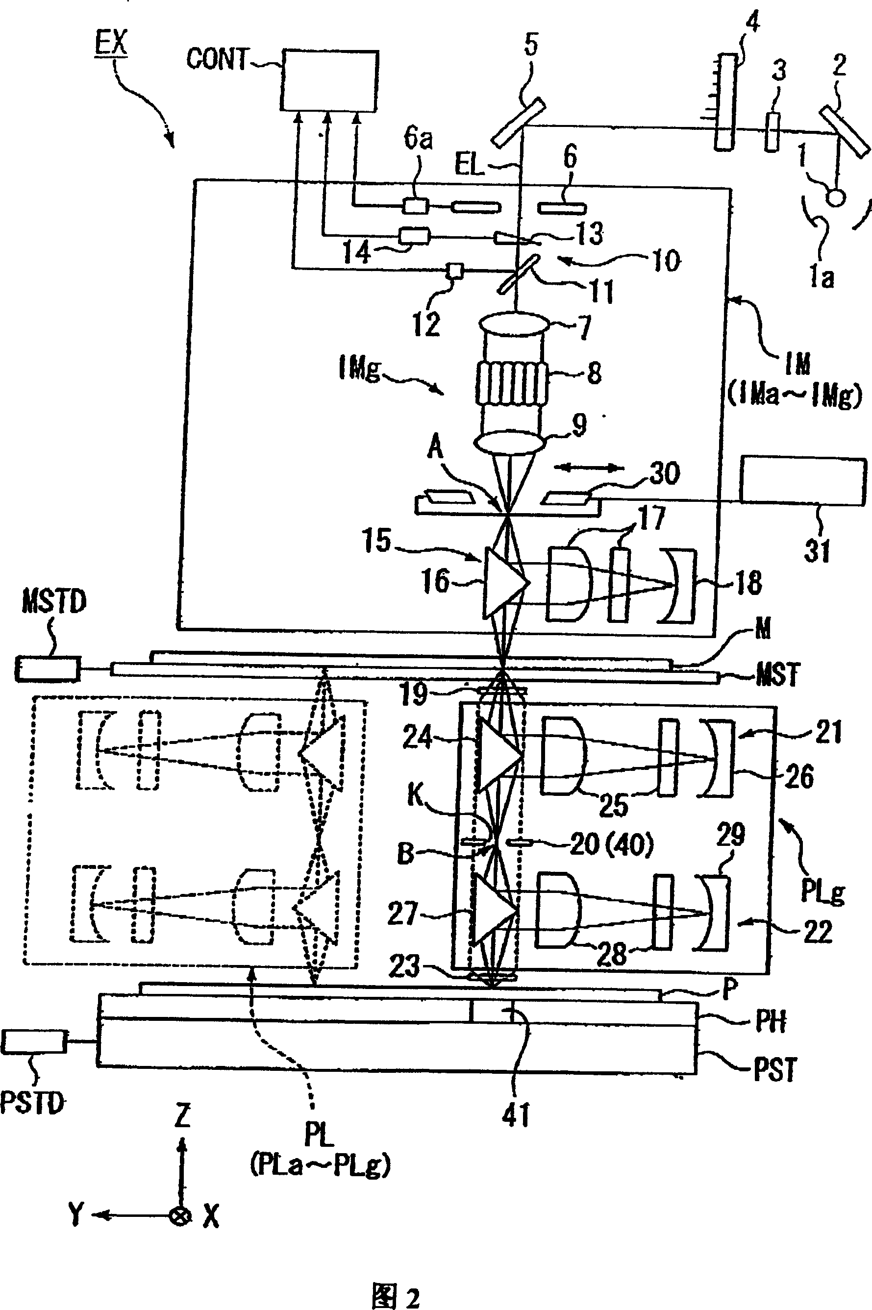
[0062] Hereinafter, the exposure apparatus and the exposure method of this invention, and the manufacturing method of the element are demonstrated with reference to drawing. FIG. 1 is a schematic perspective view of an embodiment of the exposure apparatus of the present invention, and FIG. 2 is a schematic configuration diagram of the exposure apparatus.

[0063] In FIGS. 1 and 2, the exposure device EX includes a mask table MST on which a mask M is placed; and an illumination optical system IL that can emit an exposure (beam) EL to illuminate the mask M on the mask table MST; and a substrate table PST , placing the photosensitive substrate P so as to expose the pattern formed on the mask M; and the projection optical system PL, projecting and exposing the pattern image of the mask M irradiated by the illumination optical system IL on the substrate stage PST. This illumination optical system IL has a plurality (seven in this embodiment) of illumination elements IM (IMa˜IMg). ...


PUM


Abstract

The present invention provides an exposure device. The device freely adjusts the sizes of patterns formed on the photo-substrate and the dividing locations of patterns on the mask when carrying out continuous exposure on divided patterns. A scan typed exposure device contains a view shutter which can set up the width of the scanning direction of the projected area (50) on the photo-substrate P. A light shield sets up the width of said projected area (50) on the photo-substrate P on the non-scanning direction. And a blind (30) moves along the non-scanning direction to define the contiguous area of the pattern shadow in order to have the cumulative exposure light in the contiguous area faded away from one side toward the edge of the lighting area.

Description

technical field [0001] The present invention relates to a scanning exposure device and an exposure method for synchronously moving a mask and a photosensitive substrate, and exposing the pattern of the mask on the photosensitive substrate, especially related to repeatedly exposing a part of adjacent patterns on the photosensitive substrate. An exposure device and an exposure method, and a method for manufacturing an element. Background technique [0002] Both liquid crystal display elements and semiconductor elements are manufactured by a so-called photolithography and etch method in which a pattern formed on a mask is transferred onto a photosensitive substrate. The exposure device used in the lithographic etching process includes a substrate stage on which a photosensitive substrate can be moved two-dimensionally, and a mask stage on which a mask with a pattern can be moved two-dimensionally. While moving the mask stage and the substrate stage one by one, the pattern form...

Claims


Application Information

Patent Timeline
Patent Type & Authority Patents(China)
IPC IPC(8): H01L21/027G03F7/20G03F7/22G03F9/00
CPCG03F7/70066
Inventor 白户章仁加藤正纪
Owner NIKON CORP
Why Eureka
Try Eureka