Single-output feedback-free sequential test response compression circuit

A technology for testing circuits and circuits, used in circuits, electronic circuit testing, electrical components, etc., to solve problems such as insufficient memory capacity, inability to keep up with testing frequency, and long testing time.

Inactive Publication Date: 2006-09-27
INST OF COMPUTING TECH CHINESE ACAD OF SCI
View PDF0 Cites 0 Cited by
  • Summary
  • Abstract
  • Description
  • Claims
  • Application Information

AI Technical Summary

Problems solved by technology

[0002] With the development of technology, especially with the development of system-level chips, more and more logic units (such as microprocessors, memories, DSPs, I / O controllers) are integrated on a single chip, and their functions are becoming more and more complex. Brings many new challenges to testing
These challenges mainly include: 1) The test frequency of the test equipment cannot keep up with the increase in chip frequency 2) The test time is too long, resulting in a substantial increase in test cost 3) The memory capacity of the test equipment is insufficient 4) The chip can be used as a test guide for full-scan designs Insufficient feet
2) The response may contain many uncertain bits
3) It must be possible to provide a simple method to collect complete diagnostic information, and this diagnosis must be without assumptions
A disadvantage of combinational circuits is that they have low compression ratios and do not provide a complete targeting solution, and their diagnosis must be based on assumptions that cannot be guaranteed
Uncertain bits cannot be completely eliminated in large-scale SOC design

Method used


Image

  • Single-output feedback-free sequential test response compression circuit
  • Single-output feedback-free sequential test response compression circuit
  • Single-output feedback-free sequential test response compression circuit

Examples


Embodiment Construction

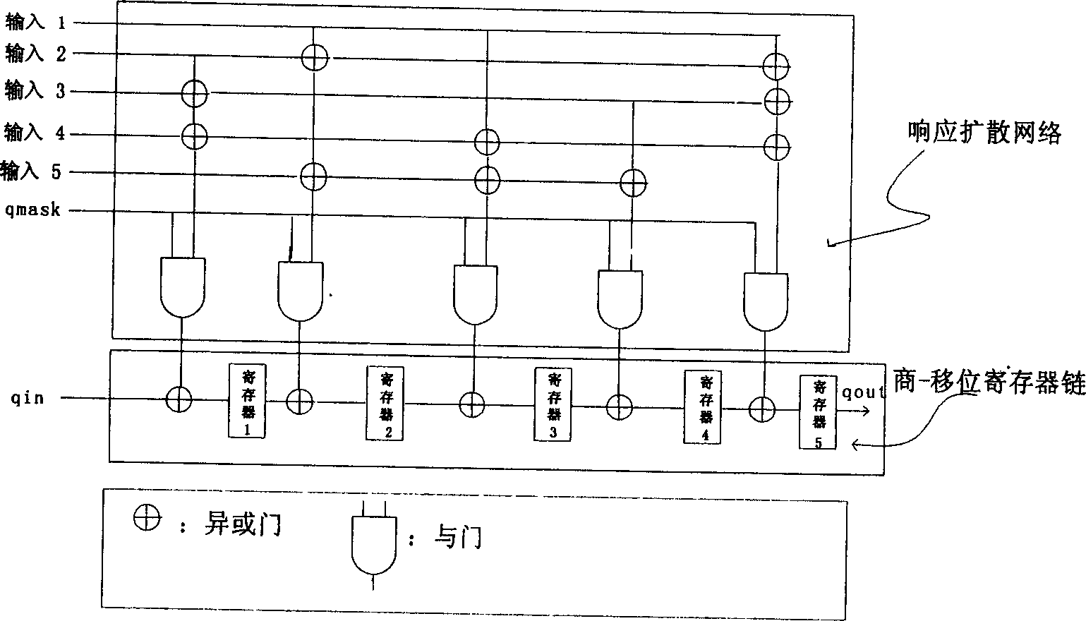
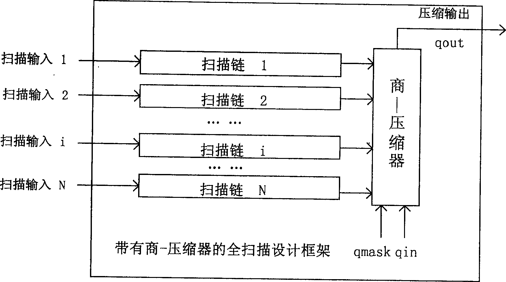
[0058] The invention is applied to compress test responses. Figure 2 depicts a full-scan design framework with a quotient-compressor. As can be seen from the figure, a responsive compressor is designed on the output of the scan chain. Compress the output of multiple scan chains into one output, and output it to the test equipment for comparison through a scan output pin. Therefore, from the perspective of the entire design process, the design of the response compressor can basically be independent of the design of the scan chain. Therefore, the insertion of the response compressor does not need to modify the design process of the original chip, nor does it need to modify the testability design process of the original chip.

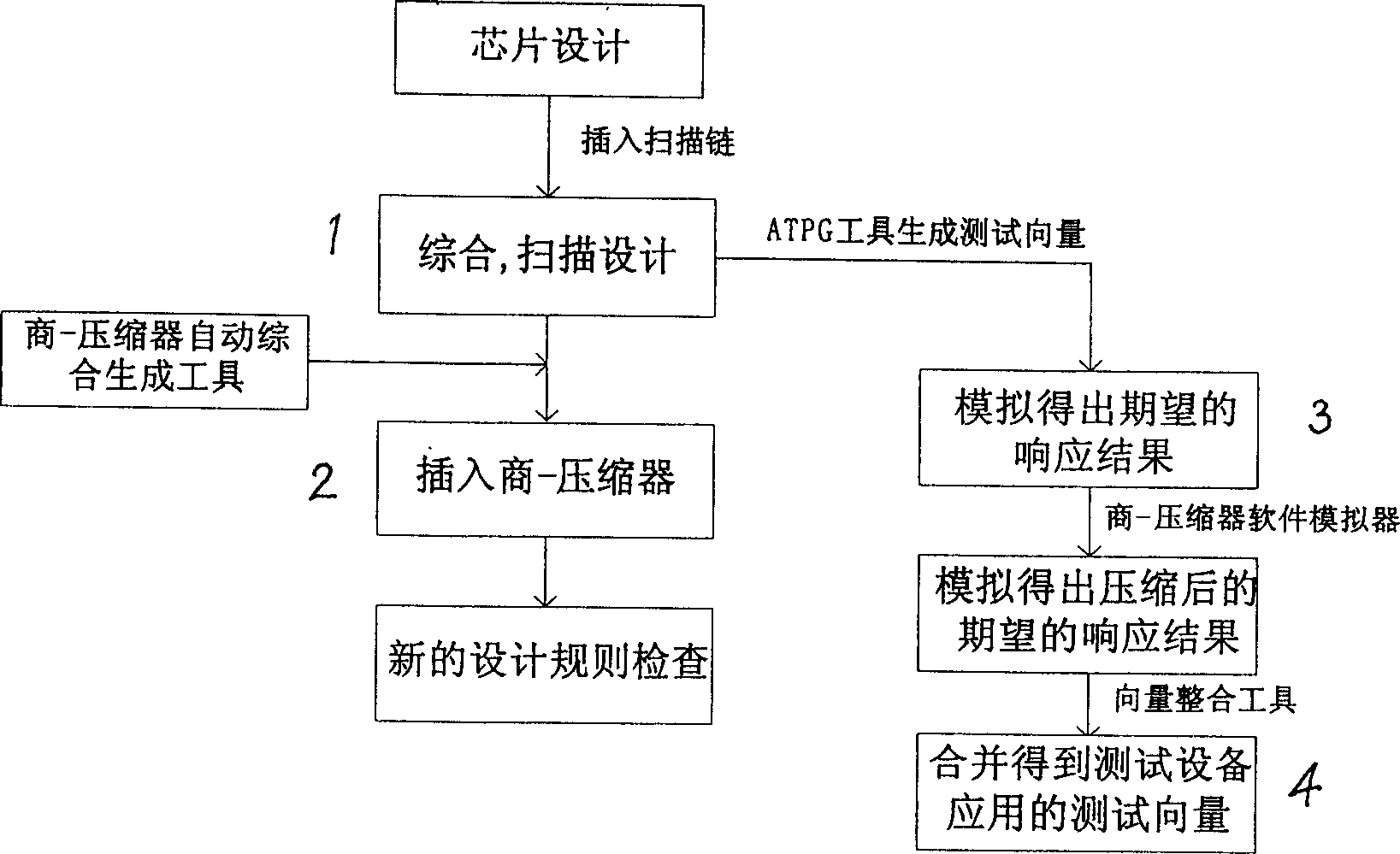
[0059] Figure 3 lists the applicator-compressor design-for-test flow. It can be seen that the testability design process for an application provider-compressor can be divided into the following steps:

[0060] 1) Synthesis, scan chain design. In this ...


PUM


Abstract

The present invention relates to a test response compressor in design of chip testability, and provides a single-output sequential comprssion circuit: quotient-compressor. Said compression circuit includes two portions: (1) response diffusion network and (2). quotient-shifting register chain. Said invention also provides three rules must be met for designing diffusion matrix correspondent to the response diffusion network, and its compression rate is high, and its testing time can be reduced, and it has no erroneous judgement.

Description

technical field [0001] The invention relates to the technical field of testability of integrated circuit chips, in particular to a single-output non-feedback sequential test response compression circuit in chip full-scan design. Background technique [0002] With the development of technology, especially with the development of system-level chips, more and more logic units (such as microprocessors, memories, DSPs, I / O controllers) are integrated on a single chip, and their functions are becoming more and more complex. It brings many new challenges to the test. These challenges mainly include: 1) The test frequency of the test equipment cannot keep up with the increase in chip frequency 2) The test time is too long, resulting in a substantial increase in test cost 3) The memory capacity of the test equipment is insufficient 4) The chip can be used as a test guide for full-scan designs Insufficient feet. A feasible solution to the lack of test pins is to compress the test re...

Claims


Application Information

Patent Timeline
Patent Type & Authority Patents(China)
IPC IPC(8): G06F7/52G01R31/28H01L23/58
Inventor 韩银和李晓维
Owner INST OF COMPUTING TECH CHINESE ACAD OF SCI
Why Eureka
Try Eureka