


Quick Research
Generate reliable direction feasibility study reports for your R&D in just a few steps.

Technical Q&A
Discover and master advanced knowledge NOW. Basics, ideas, possibilities, all at once.

Find Solutions
As an expert in R&D theories, this can generate solutions to your technical problems instantly.

Evaluate Feasibility
Analyze your overall solution with one click, know your potential R&D risks in advance.

Monitor Landscape
Get weekly tech updates, stay abreast of the latest tech innovations and key insights.
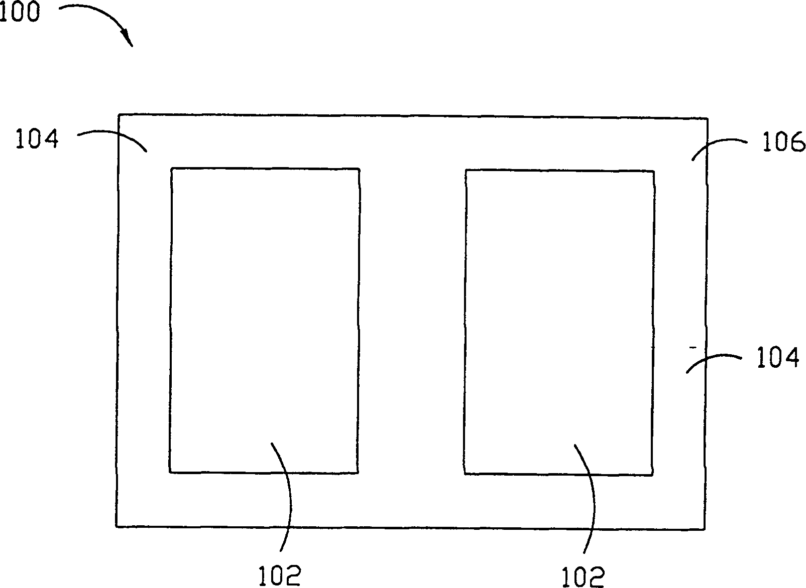
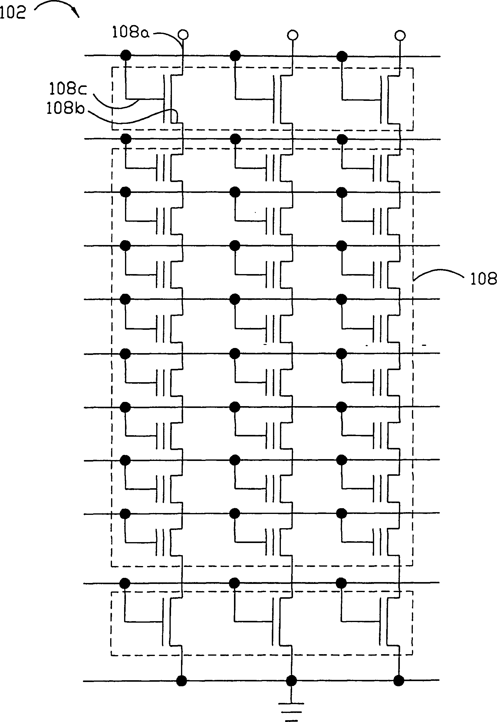
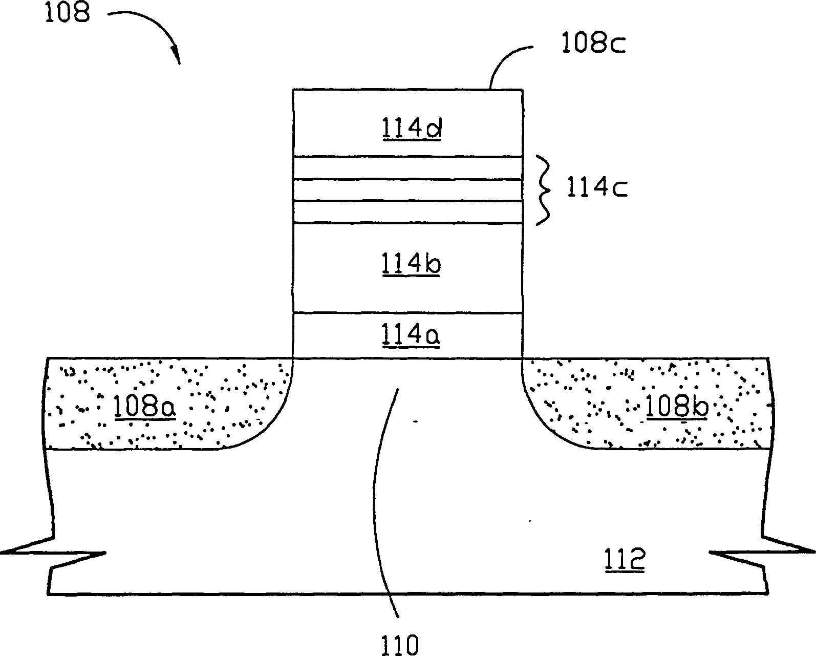
High-performance grid nitride ROM structure
A gate structure, silicon nitride layer technology, applied in the direction of electric solid devices, semiconductor devices, electrical components, etc., can solve the problems of high local electric field, low reliability, low gate oxide accumulation and so on
- Summary
- Abstract
- Description
- Claims
- Application Information
AI Technical Summary
Problems solved by technology
Method used
Image

Examples
Embodiment Construction
[0022] The present invention can be widely applied to many semiconductor devices, and can be produced by using many different semiconductor materials. When the present invention describes the structure of the present invention with a preferred embodiment, the existing people in this field should have the cognition Many steps and materials can be replaced, and these general replacements undoubtedly do not depart from the spirit of the present invention and the scope of claims.
[0023] Secondly, the present invention is described in detail as follows with schematic diagrams. When describing the embodiments of the present invention in detail, the cross-sectional view showing the semiconductor structure will not be partially enlarged according to the general scale in the semiconductor manufacturing process for the convenience of explanation, but it should not be used as a limited definition. Know. In addition, in actual production, the three-dimensional space dimensions of length...
PUM
| Property | Measurement | Unit |
|---|---|---|
| thickness | aaaaa | aaaaa |
| thickness | aaaaa | aaaaa |
| thickness | aaaaa | aaaaa |
Abstract
Description
Claims
Application Information
 - R&D Engineer
- R&D Manager
- IP Professional
- Industry Leading Data Capabilities
- Powerful AI technology
- Patent DNA Extraction
Browse by: Latest US Patents, China's latest patents, Technical Efficacy Thesaurus, Application Domain, Technology Topic, Popular Technical Reports.
© 2024 PatSnap. All rights reserved.Legal|Privacy policy|Modern Slavery Act Transparency Statement|Sitemap|About US| Contact US: help@patsnap.com