Manufacturing method of copper-embedded circuit board

A production method and circuit board technology, applied in the direction of multi-layer circuit manufacturing, etc., can solve the problems of slow operation, easy leakage or displacement, and easy error, and achieve the effect of accurate embedding position

Pending Publication Date: 2022-08-05
广东依顿电子科技股份有限公司
View PDF0 Cites 0 Cited by
  • Summary
  • Abstract
  • Description
  • Claims
  • Application Information

AI Technical Summary

Problems solved by technology

[0004] 1. The operation of manually placing copper blocks is slow, especially when dozens or even hundreds of copper blocks need to be placed in the circuit board, it takes a lot of manpower and time, which greatly affects the work efficiency of buried copper circuit boards; 2. It is impossible Effectively prevent the risk of leakage; 3. After the copper block is placed in the copper block slot, other actions will occur, such as the risk of leakage or displacement during the stacking or plate transfer process; 4. Like a circuit board with different shapes, When embedding copper blocks of different sizes, manual operation will be more error-prone

Method used


Image

  • Manufacturing method of copper-embedded circuit board
  • Manufacturing method of copper-embedded circuit board
  • Manufacturing method of copper-embedded circuit board

Examples


Embodiment Construction

[0037] The technical solutions of the present invention will be described in detail below with reference to the drawings.

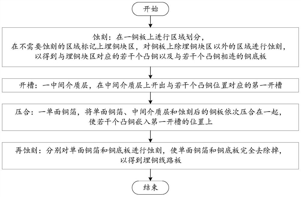
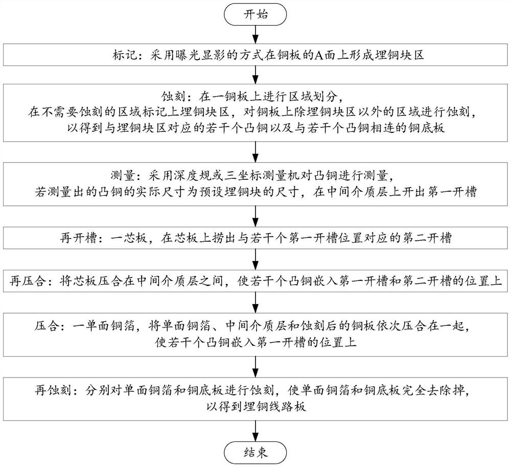
[0038] see Figure 1 to Figure 10 , the manufacturing method of the buried copper circuit board of this embodiment includes the following steps:

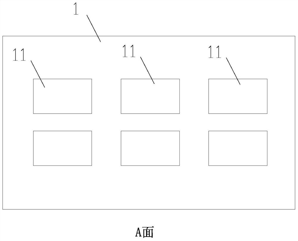
[0039] Etching: perform area division on a copper plate 1, mark the buried copper block area 11 on the area that does not need to be etched, and etch the area on the copper plate 1 except the buried copper block area 11 to obtain the buried copper block area 11. A number of bump copper 12 and a copper base plate 13 connected to a number of bump copper 12;

[0040] Slotting: an intermediate dielectric layer 2, on which a first slot 21 corresponding to the positions of several protruding coppers 12 is opened;

[0041] Pressing: a single-sided copper foil 3, the single-sided copper foil 3, the intermediate dielectric layer 2 and the etched copper plate 1 are pressed together in turn, so that several convex coppe...


PUM

PropertyMeasurementUnit
thicknessaaaaaaaaaa

Abstract

The invention provides a manufacturing method of a copper-embedded circuit board, which comprises the following steps of: etching: carrying out region division on a copper plate, marking a copper block embedding region on a region which does not need to be etched, and etching the region, except the copper block embedding region, on the copper plate to obtain a plurality of pieces of convex copper corresponding to the copper block embedding region and a copper bottom plate connected with the plurality of pieces of convex copper; grooving: forming first grooves corresponding to the convex copper parts in position on the middle dielectric layer; pressing: sequentially pressing the single-sided copper foil, the middle dielectric layer and the etched copper plate together, and embedding the plurality of convex copper into the position of the first slot; and re-etching: etching the single-sided copper foil and the copper bottom plate respectively to completely remove the single-sided copper foil and the copper bottom plate so as to obtain the copper-embedded circuit board. According to the manufacturing method of the copper-embedded circuit board provided by the invention, a plurality of copper blocks with different shapes and different sizes can be embedded at one time, and meanwhile, the embedding positions of the copper blocks are ensured to be accurate and other risks of missing placement and falling are avoided.

Description

technical field [0001] The invention relates to the technical field of circuit boards, in particular to a manufacturing method of a buried copper circuit board. Background technique [0002] At present, for burying copper blocks with a size below 10*10mm, the existing technology mostly adopts manual placement, that is, manually burying the copper blocks in the pre-etched copper block grooves, and then pressing them together. [0003] However, in practice, it is found that most of the existing methods for making buried copper circuit boards have the following problems: [0004] 1. The operation of manually placing copper blocks is slow, especially when dozens or even hundreds of copper blocks need to be placed in the circuit board, it takes a lot of manpower and time, which greatly affects the work efficiency of buried copper circuit board production; 2. It is impossible to Effectively prevent the risk of leakage; 3. After the copper block is placed in the copper block slot,...

Claims


Application Information

Patent Timeline
Patent Type & Authority Applications(China)
IPC IPC(8): H05K3/46
CPCH05K3/4697H05K2201/10416
Inventor 邱小华
Owner 广东依顿电子科技股份有限公司
Why Eureka
Try Eureka