Wafer structure for bonding and forming method and bonding method thereof

A wafer and bonding technology, used in semiconductor/solid-state device parts, semiconductor devices, electrical components, etc., can solve problems such as bubbles and film thickness deviation, and achieve the effect of improving device reliability and avoiding bubble defects

Pending Publication Date: 2022-08-05
SEMICONDUCTOR MANUFACTURING INTERNATIONAL (BEIJING) CORP +1
View PDF0 Cites 0 Cited by
  • Summary
  • Abstract
  • Description
  • Claims
  • Application Information

AI Technical Summary

Problems solved by technology

[0004] CMP can cause film thickness deviation, and film thickness deviation can cause bubble defects after wafer bonding

Method used


Image

  • Wafer structure for bonding and forming method and bonding method thereof
  • Wafer structure for bonding and forming method and bonding method thereof
  • Wafer structure for bonding and forming method and bonding method thereof

Examples


Embodiment Construction

[0026] The following description provides specific application scenarios and requirements of the present application, and is intended to enable those skilled in the art to make and use the contents of the present application. Various partial modifications to the disclosed embodiments will be readily apparent to those skilled in the art, and the generic principles defined herein may be applied to other embodiments and without departing from the spirit and scope of the present application. application. Therefore, the present application is not to be limited to the embodiments shown, but is to be accorded the widest scope consistent with the claims.

[0027] The technical solutions of the present invention will be described in detail below with reference to the embodiments and the accompanying drawings.

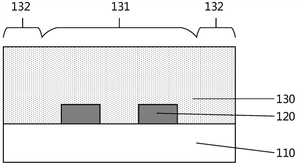
[0028] During wafer bonding, a dielectric layer is formed on the surface of the wafer to make bonding marks. The dielectric layer needs to be sufficiently flat, so the dielect...


PUM


Abstract

The invention provides a wafer structure for bonding and a forming method and a bonding method thereof. The bonding method comprises the following steps: providing a first wafer and a second wafer; and aligning the first wafer and the second wafer by using the first mark area and carrying out bonding. According to the wafer structure for bonding and the forming method and the bonding method thereof, the thickness of the edge of the wafer is smaller than the thickness of the center of the wafer, the bubble defect generated after wafer bonding can be avoided, and the reliability of a device is improved.

Description

technical field [0001] The present application relates to the field of semiconductor technology, and in particular, to a wafer structure for bonding, a method for forming the same, and a method for bonding. Background technique [0002] During the wafer bonding process, if the edges of the wafers are in contact with each other in advance, the wafers will form a closed loop in advance, resulting in the inability of the gas between the wafers to be evacuated normally, resulting in the formation of bubble defects at the edges of the wafers. The main reasons for the early contact of the wafer edge include the following two: one is the process fluctuation, such as the fluctuation of the thickness of the bonding medium film; the other is the warpage of the wafer, which causes the overall unevenness of the wafer and the early contact of the edge. [0003] The fluctuation of the film thickness of the bonding medium on the wafer surface can be caused by the chemical mechanical polish...

Claims


Application Information

Patent Timeline
Patent Type & Authority Applications(China)
IPC IPC(8): H01L21/68H01L23/544H01L21/18
CPCH01L21/682H01L23/544H01L21/185H01L2223/54426
Inventor 刘清召
Owner SEMICONDUCTOR MANUFACTURING INTERNATIONAL (BEIJING) CORP
Why Eureka
Try Eureka