
Clock synchronization method, device, system and equipment for chip testing

A clock synchronization and chip testing technology, applied in digital circuit testing, electronic circuit testing, etc., can solve the problems of long test time, occupation, slow SPI interface configuration, etc., to achieve low cost, fast configuration, and reduced area Effect

Pending Publication Date: 2022-08-02
SUZHOU HUAXING YUANCHUANG TECH CO LTD
View PDF0 Cites 2 Cited by
  • Summary
  • Abstract
  • Description
  • Claims
  • Application Information

AI Technical Summary

Problems solved by technology

The slow speed of SPI interface configuration results in longer test time; the dedicated clock chip occupies the I / O (Input / Output, input / output) pin resources of the FPGA (Field Programmable Gate Array, and the PCB) (Printed Circuit Board, printed circuit board) design area increases the design complexity and design cost of the system

Method used

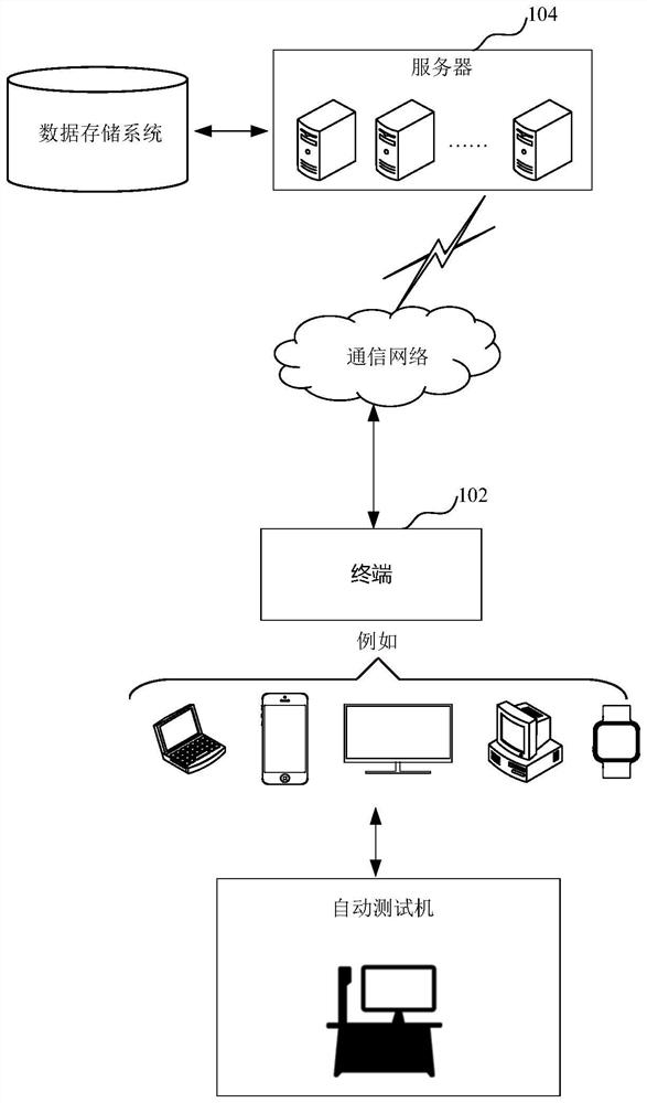
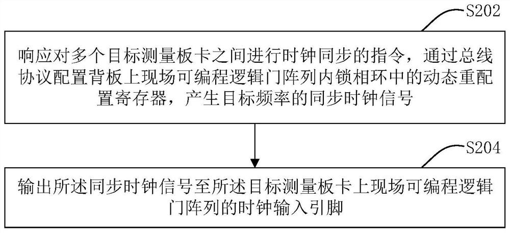
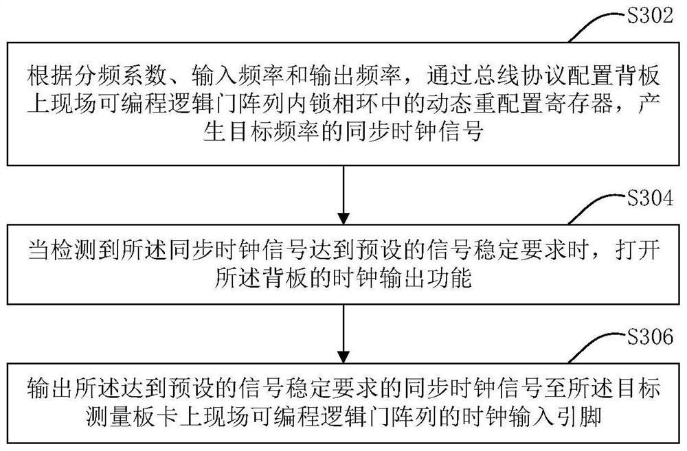

Image

  • Clock synchronization method, device, system and equipment for chip testing
  • Clock synchronization method, device, system and equipment for chip testing
  • Clock synchronization method, device, system and equipment for chip testing

Examples


Embodiment Construction

[0040] In order to make the objectives, technical solutions and advantages of the present disclosure more clear, the present disclosure will be further described in detail below with reference to the accompanying drawings and embodiments. It should be understood that the specific embodiments described herein are only used to explain the present disclosure, but not to limit the present disclosure.

[0041] It should be noted that when an element is referred to as being "fixed to" another element, it can be directly on the other element or intervening elements may also be present. When an element is referred to as being "connected" to another element, it can be directly connected to the other element or intervening elements may also be present. As used herein, the terms "vertical", "horizontal", "left", "right", "upper", "lower", "front", "rear", "circumferential" and similar expressions are The orientation or positional relationship shown in the figures is only for the conveni...


PUM


Abstract

The invention relates to a clock synchronization method, device, system and equipment for chip testing. The method comprises the following steps: generating a synchronous clock signal of a target frequency by responding to an instruction for carrying out clock synchronization among a plurality of target measurement board cards and configuring a dynamic reconfiguration register in a phase-locked loop in a field programmable logic gate array on a backboard through a bus protocol; and outputting the synchronous clock signal to a clock input pin of a field programmable logic gate array on the target measurement board card. According to the embodiment of the invention, the dynamic reconfiguration register in the existing phase-locked loop on the backboard is utilized to output the synchronous clock signals to a plurality of target measurement board cards at the same time, and a special clock chip is not needed; and the dynamic reconfiguration register in the phase-locked loop is configured through the bus protocol, so that the configuration speed is high, the cost is low, input / output pins in the field programmable logic gate array are not occupied, and the area of a printed circuit board is reduced.

Description

technical field [0001] The present disclosure relates to the technical field of chip testing, and in particular, to a clock synchronization method, apparatus, system and device for chip testing. Background technique [0002] The digital chip tester usually uses the pattern (sequence characteristic) test to judge whether the chip function is normal, so as to realize the rapid test when the digital chip is mass-produced. The digital chip tester generally supports hundreds of pattern test channels, such as 512, 768, 1024 channels, etc. The pattern digital waveform output by each channel needs to be output to the pins of the digital chip to be tested at the same time, that is, the pattern digital waveform needs an edge Alignment to ensure that the timing between the signals output to the pins of the digital chip under test is correct. To ensure that the digital waveforms output by all pattern channels of all digital chip testers are edge-aligned, the clocks of each digital meas...

Claims


Application Information

Patent Timeline
IPC IPC(8): G01R31/317
CPCG01R31/31726
Inventor 董亚明韩洁
Owner SUZHOU HUAXING YUANCHUANG TECH CO LTD
Learn More