PCB polishing device for mechano-electronic engineering

A PCB board and mechatronics technology, which is applied in the field of PCB board polishing devices for mechatronics engineering, can solve the problems of physical injury of workers, polishing dust polluting the workshop, and low polishing dust treatment effect, so as to achieve the effect of reducing pollution

Inactive Publication Date: 2022-07-29
SUQIAN COLLEGE
View PDF0 Cites 0 Cited by
  • Summary
  • Abstract
  • Description
  • Claims
  • Application Information

AI Technical Summary

Problems solved by technology

[0003] The PCB board needs to be polished during processing. The traditional polishing device handles the polishing dust by directly installing an exhaust fan to discharge the internal dust. The processing effect on the polishing dust is relatively low, and the discharged polishing dust will pollute the work. Workshop, causing injury to workers; therefore, we designed a PCB board polishing device for mechanical and electronic engineering to solve the above problems

Method used


Image

  • PCB polishing device for mechano-electronic engineering
  • PCB polishing device for mechano-electronic engineering
  • PCB polishing device for mechano-electronic engineering

Examples


Embodiment Construction

[0025] The technical solutions in the embodiments of the present invention will be clearly and completely described below with reference to the accompanying drawings in the embodiments of the present invention. Obviously, the described embodiments are only a part of the embodiments of the present invention, but not all of the embodiments.

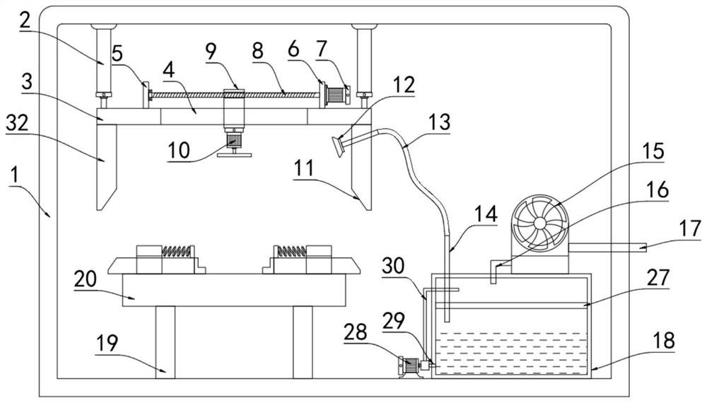
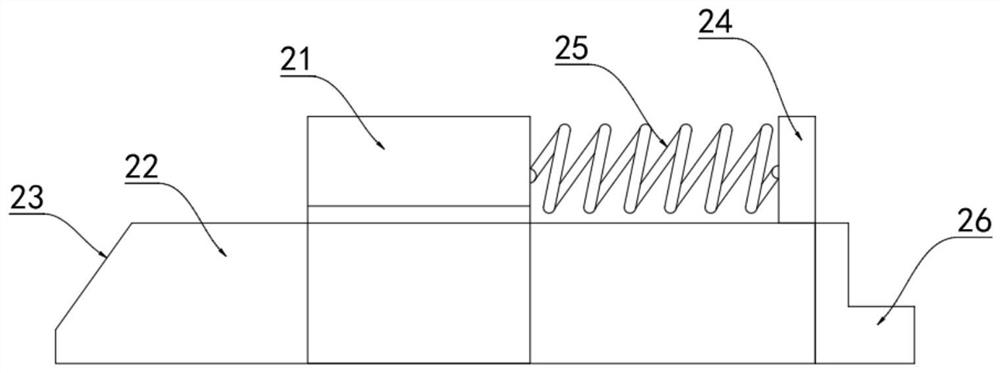
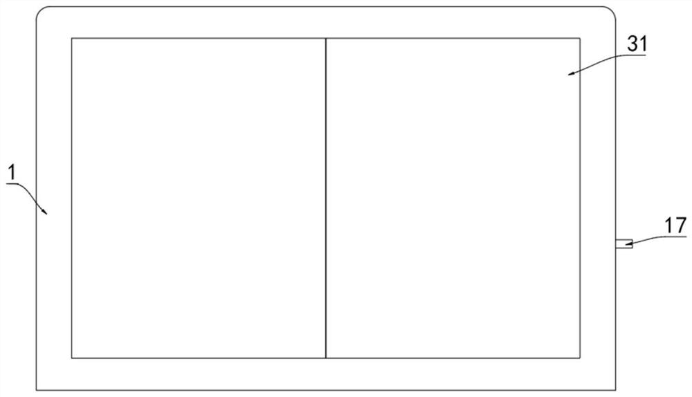
[0026] refer to Figure 1-4 , a PCB board polishing device for mechanical and electronic engineering, including a box body 1, the box body 1 is provided with ventilation holes, which are not shown in the figure; the front end of the box body 1 is installed with two switch doors 31, The hinge is connected with the box body 1; the box body 1 is provided with a movable plate 3, and two electric push rods 2 are arranged between the movable plate 3 and the inner top of the box body 1, and the fixed end of the electric push rod 2 is connected to the box body 1. The inner top of the electric push rod 2 is fixedly connected, and the output end of t...


PUM


Abstract

The PCB polishing device for mechanical electronic engineering comprises a box body, a moving plate is arranged in the box body, two electric push rods are arranged between the moving plate and the inner top of the box body, a sliding block which is in sliding connection with the moving plate is arranged in the middle of the moving plate in an up-down penetrating mode, and a polishing machine is installed at the bottom of the sliding block. And a driving mechanism is arranged between the sliding block and the moving plate, driving plates are installed at the bottoms of the two ends of the moving plate, first inclined faces are arranged at the lower ends of the opposite faces of the two driving plates, and four supporting rods are installed at the inner bottom of the box body. By means of work of an electric push rod, the polishing machine can move downwards, meanwhile, two L-shaped plates can be driven to move relatively, a PCB is clamped, the polishing machine moves in a reciprocating mode under transmission of a lead screw, the surface of the PCB can be polished, meanwhile, dust generated during polishing can be sucked into a water tank, and the dust is treated and collected; and the pollution to the workshop environment is reduced.

Description

technical field [0001] The invention relates to the technical field of PCB board processing, in particular to a PCB board polishing device for mechanical and electronic engineering. Background technique [0002] PCB, the Chinese name is printed circuit board, also known as printed circuit board, is an important electronic component, a support body for electronic components, and a carrier for electrical connection of electronic components. Because it is made using electronic printing, it is called a "printed" circuit board. [0003] The PCB board needs to be polished during processing. The traditional polishing device handles the polishing dust by directly installing an exhaust fan to discharge the internal dust. The treatment effect of the polishing dust is relatively low, and the discharged polishing dust will pollute the work. workshop, causing injuries to workers' bodies; therefore, we designed a PCB board polishing device for mechanical and electronic engineering to sol...

Claims


Application Information

Patent Timeline
Patent Type & Authority Applications(China)
IPC IPC(8): B24B29/02B24B41/06B24B47/22B24B47/16B24B55/06B24B55/12
CPCB24B29/02B24B41/06B24B47/22B24B47/16B24B55/06B24B55/12
Inventor 邱义臻李守军孙延永
Owner SUQIAN COLLEGE
Why Eureka
Try Eureka