Photoelectric detector and preparation method thereof
A photodetector and injector technology, applied in the field of photodetectors, can solve the problems of low quantum efficiency and responsivity, wide band gap, etc., and achieve the effects of improving quantum luminescence efficiency, reducing recombination rate, and simple manufacturing process
- Summary
- Abstract
- Description
- Claims
- Application Information
AI Technical Summary
Problems solved by technology
Method used
Image

Examples
Embodiment Construction
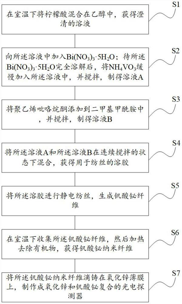
[0027] The specific embodiments of the present invention will be further described in detail below with reference to the embodiments and the accompanying drawings. Here, the following examples of the present invention are used to illustrate the present invention, but not to limit the scope of the present invention.
[0028] An embodiment of the present invention provides a photodetector, comprising: a zinc oxide film and a bismuth vanadate nanofiber compounded on the zinc oxide film. Bismuth vanadate nanofibers are discretely composited on ZnO films by drop casting.
[0029] In the photodetector provided by the invention, the bismuth vanadate nanofibers are dispersed discretely on the zinc oxide film. Since bismuth vanadate is also an N-type semiconductor with a direct bandgap, it has a narrow bandgap in the range of 2.4–2.6 eV with photoresponsiveness in the visible and near-infrared range. Its composite with ZnO thin films provided sufficient ZnO surface area to interact w...
PUM
 Abstract
Description
Claims
Application Information
 - R&D
- Intellectual Property
- Life Sciences
- Materials
- Tech Scout
- Unparalleled Data Quality
- Higher Quality Content
- 60% Fewer Hallucinations
Browse by: Latest US Patents, China's latest patents, Technical Efficacy Thesaurus, Application Domain, Technology Topic, Popular Technical Reports.
© 2025 PatSnap. All rights reserved.Legal|Privacy policy|Modern Slavery Act Transparency Statement|Sitemap|About US| Contact US: help@patsnap.com