Hot carrier solar cell and photovoltaic module
A technology of solar cells and hot carriers, which is applied in the direction of electrical components, electric solid devices, circuits, etc., can solve the problems of less sunlight absorption and limited hot carrier efficiency improvement of solar cells
- Summary
- Abstract
- Description
- Claims
- Application Information
AI Technical Summary
Problems solved by technology
Method used
Image
Examples
Embodiment 1
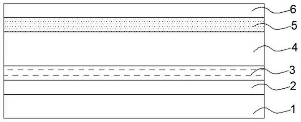
[0071] In this embodiment, the hot carrier solar cell includes a substrate, a first electrode, a first hot carrier transport layer, a light absorption layer, a second hot carrier transport layer, and a second electrode.
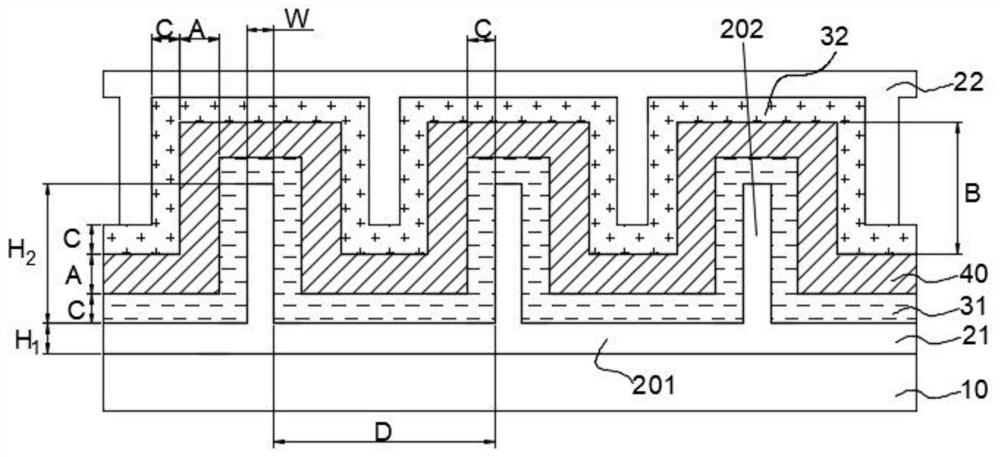
[0072] In this embodiment, sunlight is incident from the substrate side. The substrate is glass. The first electrode is made of FTO material, in which H 1 =500nm, H 2 =500nm, W=200nm, D=2000nm. The first hot carrier transport layer transports hot electrons, which adopts Bphen material and has a thickness of 100 nm. The light absorbing layer is FAPbI 3 The light absorption layer composed of perovskite quantum dots has a thickness of 200 nm, and the size of the quantum dots constituting the light absorption layer is 6 nm. The second hot carrier transport layer transports hot holes, adopts CBP material, and has a thickness of 100 nm. The second electrode is made of Au material, where H 1 =500nm, H 2 =500nm, W=200nm, D=2000nm. The second electrodes are a...
Embodiment 2
[0074] In this embodiment, the hot carrier solar cell includes a substrate, a first electrode, a first hot carrier transport layer, a light absorption layer, a second hot carrier transport layer, and a second electrode.
[0075] In this embodiment, sunlight is incident from the second electrode side. The substrate is glass. The first electrode is made of Ag material, in which H 1 =300nm, H 2 =600nm, W=100nm, D=1800nm. The first hot carrier transport layer transports hot electrons, which adopts TPBi material and has a thickness of 50 nm. The light absorbing layer is FAPbI 3 The light absorption layer composed of perovskite quantum dots has a thickness of 200 nm, and the size of the quantum dots constituting the light absorption layer is 6 nm. The second hot carrier transport layer transports hot holes and adopts F8 material with a thickness of 60 nm. The second electrode is made of ITO material, in which H 1 =300nm, H 2 =600nm, W=100nm, D=1800nm. The second electrodes ...
Embodiment 3
[0077] In this embodiment, the hot carrier solar cell includes a substrate, a first electrode, a first hot carrier transport layer, a light absorption layer, a second hot carrier transport layer, and a second electrode.
[0078] In this embodiment, sunlight is incident from the second electrode side. The substrate is an aluminum substrate, and the arrangement of the remaining layers is the same as that of the second embodiment. The aluminum substrate can be used as a flat electrode, and together with the first electrode, the thermal electrons can be extracted.
PUM
| Property | Measurement | Unit |
|---|---|---|
| height | aaaaa | aaaaa |
| thickness | aaaaa | aaaaa |
| thickness | aaaaa | aaaaa |
Abstract
Description
Claims
Application Information
 - R&D
- Intellectual Property
- Life Sciences
- Materials
- Tech Scout
- Unparalleled Data Quality
- Higher Quality Content
- 60% Fewer Hallucinations
Browse by: Latest US Patents, China's latest patents, Technical Efficacy Thesaurus, Application Domain, Technology Topic, Popular Technical Reports.
© 2025 PatSnap. All rights reserved.Legal|Privacy policy|Modern Slavery Act Transparency Statement|Sitemap|About US| Contact US: help@patsnap.com


