Wafer defect detection device based on automatic optical detection

An automatic optical detection and defect detection technology, which is applied in the direction of optical testing of defects/defects, measurement devices, and material analysis through optical means, can solve the problems of difficult adjustment of wafer adjustment angle and affecting the normal observation efficiency of wafers, etc. , to achieve the effect of accurate detection work

Pending Publication Date: 2022-06-17
苏州中巨苏智能科技有限公司
View PDF0 Cites 0 Cited by
  • Summary
  • Abstract
  • Description
  • Claims
  • Application Information

AI Technical Summary

Problems solved by technology

[0005] In order to solve the above-mentioned technical problems, the present invention provides a wafer defect detection device based on automatic optical detection to solve the existing need to manually replace the lampshade duri

Method used


Image

  • Wafer defect detection device based on automatic optical detection
  • Wafer defect detection device based on automatic optical detection
  • Wafer defect detection device based on automatic optical detection

Examples


Example Embodiment

[0026]实施例:

[0027]如附图1至附图4所示:

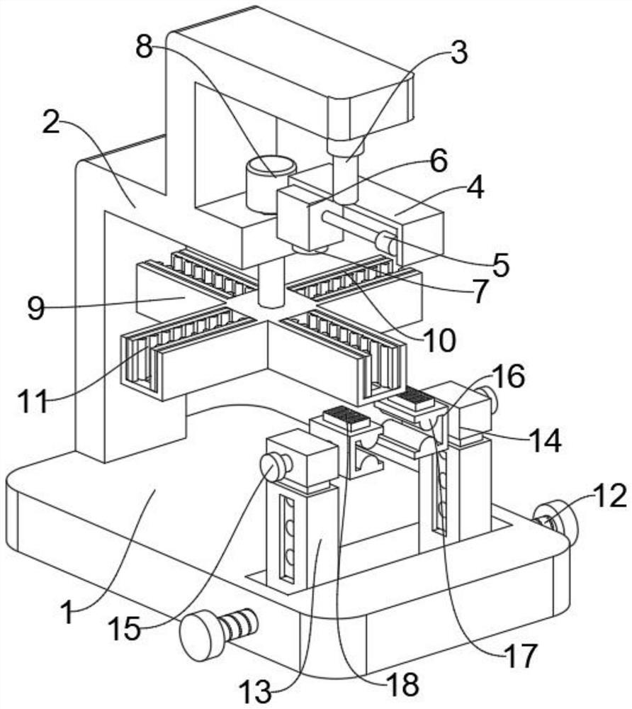
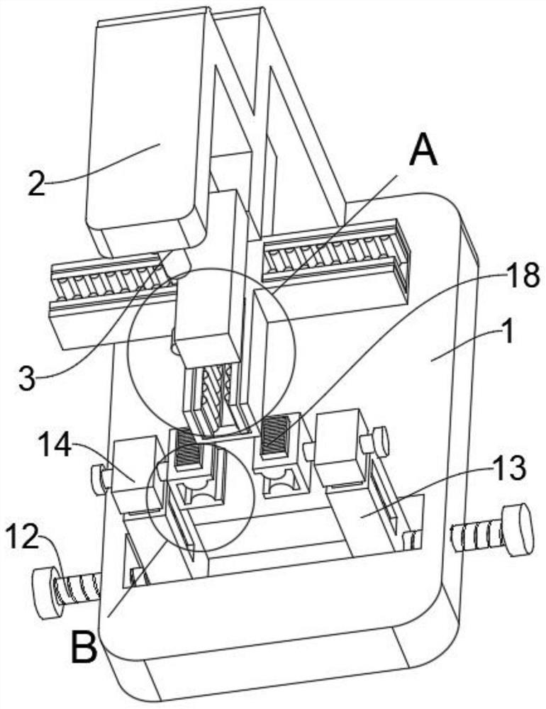
[0028]本发明提供一种基于自动光学检测的晶圆缺陷检测装置,包括底座1,底座1的主体为矩形结构,且底座1的顶端面上开设有横向槽,并且底座1中所开设的横向槽用于滑动连接有移动座13,底座1的顶端面上固定连接有支架2,支架2中横向构件的底侧安装有电动推杆A3,电动推杆A3的底端安装有导座4,导座4的内部开设有凹槽,且导座4中所开设的凹槽内部安装有电动推杆B5,电动推杆B5的另一端安装有移动块6,电动推杆B5与移动块6共同组成了调节结构,角度杆15的一侧安装有限位架16,限位架16用于限位晶圆,且每处限位架16的内部呈对向安装有两处限位气囊17,限位气囊17用于限位晶圆,限位架16的顶端安装有泵机18,泵机18用于向限位气囊17供气。

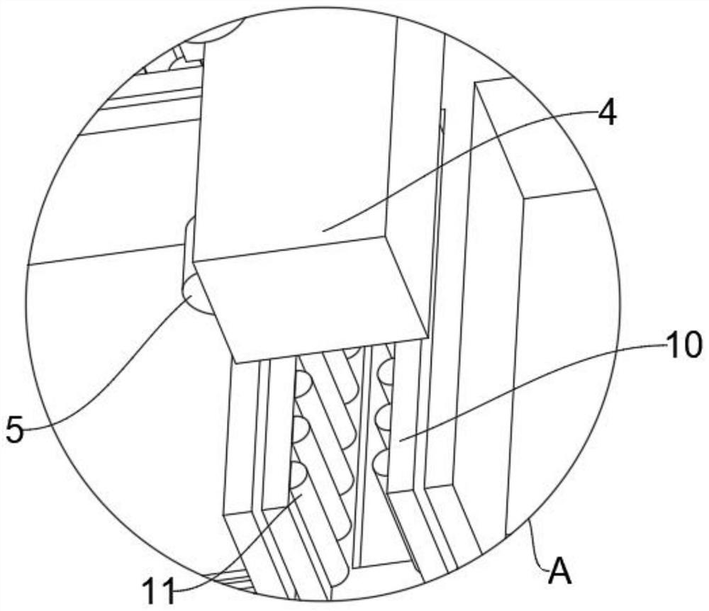
[0029]参考图1-图2,移动块6的底端安装有照射灯7,照射灯7用于罩设晶圆,支架2的内部安装有电机8,电机8的底端设置有传动轴,且传动轴穿过支架2,并凸出支架2,电机8的底侧安装有承载架9,承载架9为十字结构,承载架9的内部开设有滑槽,且承载架9的底端为贯通结构,并且承载架9的内部安装有侧板10,侧板10与承载架9之间通过弹簧连接,且侧板10中远离承载架9的一侧还呈直线阵列安装有导轮11,导轮11用于导向镜头,通过启动安装在支架2底侧的电动推杆A3将照射灯7向下推动,并通过照射灯7与放置在承载架9内部的灯罩进行连接后对限位在限位架16内部的晶圆片进行照射工作即可,并且在进行照射工作时,可以通过手动转动安装在支撑杆14外侧的角度杆15来对晶圆的翻转角度进行调整,通过主动调整照射灯7照射到晶圆之上的角度变化即可对晶圆片的缺陷进行快速的检测工作。

[0030]参考图1-图4,底座1中所开设的横向槽的内部滑动连接有移动座13,底座1的外侧安装有调节杆12,调节杆12共设有两处,且两处调节杆12分别拧接在底座1的左右两侧位置,并且调节杆12用于调节移动座13在底座1中横向槽的位置,移动座13为内部中空结构,且移动座13的外侧开设有通槽,并且移动座13的内部插接有支撑杆14,支撑杆14的内部呈直线阵列开设有通孔,并且支撑杆14中所开设的通孔用于安装限位销,支撑杆14的内部转动连接有角度杆15,在当需要进行照射工作时,可以通过将不同规格的灯罩放入到承载架9的内部位置,并通过安装在承载架9内侧的...


PUM


Abstract

The invention provides a wafer defect detection device based on automatic optical detection, and relates to the technical field of wafer defect detection.The wafer defect detection device comprises a base, a main body of the base is of a rectangular structure, a transverse groove is formed in the top end face of the base, and the transverse groove formed in the base is used for being slidably connected with a movable base; a support is fixedly connected to the top end face of the base, and the problems that in the prior art, a lampshade needs to be replaced manually in the detection process, then the normal observation efficiency of a wafer is affected, and when the wafer is grabbed manually to adjust the angle in the detection process, accurate adjustment is difficult are solved. The defect of the wafer can be rapidly detected by actively adjusting the change of the angle of the irradiation lamp irradiating the wafer, and by means of the design, accurate scale adjustment is carried out on the overturning angle of the wafer, so that the wafer can be detected more accurately and more accurately.

Description

technical field [0001] The invention belongs to the technical field of wafer defect detection, and more specifically relates to a wafer defect detection device based on automatic optical detection. Background technique [0002] High-purity polysilicon is dissolved and mixed with silicon crystal seeds, and then slowly pulled out to form cylindrical monocrystalline silicon. After the silicon crystal rod is ground, polished, and sliced, it forms a silicon wafer, that is, a wafer. In the process of production, some surface defects will be produced due to the difference in technology, which needs to be tested after being illuminated by light. [0003] However, most of the existing detection devices need to manually replace the lampshades of different colors to realize that the detection light emitted by the lamp emits white light or yellow-green light to irradiate the wafer, and the wafer is manually held and turned to different angles. The inspection can only be carried out by ...

Claims


Application Information

Patent Timeline
IPC IPC(8): G01N21/01G01N21/95
CPCG01N21/01G01N21/9501
Inventor 叶井飞
Owner 苏州中巨苏智能科技有限公司
Why Eureka
Try Eureka